

DISTRIBUTION STATEMENT A: Approved for public release; distribution is unlimited.
NONRESIDENT TRAINING COURSE
SEPTEMBER 1998
Navy Electricity and Electronics Training Series
Module 13—Introduction to Number Systems and Logic NAVEDTRA 14185
DISTRIBUTION STATEMENT A: Approved for public release; distribution is unlimited.
Although the words “he,” “him,” and “his” are used sparingly in this course to enhance communication, they are not intended to be gender driven or to affront or discriminate against anyone.
i
PREFACE By enrolling in this self-study course, you have demonstrated a desire to improve yourself and the Navy. Remember, however, this self-study course is only one part of the total Navy training program. Practical experience, schools, selected reading, and your desire to succeed are also necessary to successfully round out a fully meaningful training program.
COURSE OVERVIEW: To introduce the student to the subject of Numbering Systems and Logic Circuits who needs such a background in accomplishing daily work and/or in preparing for further study.
THE COURSE: This self-study course is organized into subject matter areas, each containing learning objectives to help you determine what you should learn along with text and illustrations to help you understand the information. The subject matter reflects day-to-day requirements and experiences of personnel in the rating or skill area. It also reflects guidance provided by Enlisted Community Managers (ECMs) and other senior personnel, technical references, instructions, etc., and either the occupational or naval standards, which are listed in the Manual of Navy Enlisted Manpower Personnel Classifications and Occupational Standards, NAVPERS 18068.
THE QUESTIONS: The questions that appear in this course are designed to help you understand the material in the text.
VALUE: In completing this course, you will improve your military and professional knowledge. Importantly, it can also help you study for the Navy-wide advancement in rate examination. If you are studying and discover a reference in the text to another publication for further information, look it up.
1998 Edition Prepared by FTCS(SS) Steven F. Reith
Published by NAVAL EDUCATION AND TRAINING
PROFESSIONAL DEVELOPMENT AND TECHNOLOGY CENTER
NAVSUP Logistics Tracking Number 0504-LP-026-8380
ii
Sailor’s Creed
“I am a United States Sailor.
I will support and defend the Constitution of the United States of America and I will obey the orders of those appointed over me.
I represent the fighting spirit of the Navy and those who have gone before me to defend freedom and democracy around the world.
I proudly serve my country’s Navy combat team with honor, courage and commitment.
I am committed to excellence and the fair treatment of all.”
iii
TABLE OF CONTENTS
CHAPTER PAGE
1. Number Systems....................................................................................................... 1-1
2. Fundamental Logic Circuits ..................................................................................... 2-1
3. Special Logic Circuits .............................................................................................. 3-1
APPENDIX
I. Glossary.................................................................................................................. AI-1
II. Logic Symbols........................................................................................................ AII-1
INDEX ......................................................................................................................... INDEX-1
iv
NAVY ELECTRICITY AND ELECTRONICS TRAINING SERIES
The Navy Electricity and Electronics Training Series (NEETS) was developed for use by personnel in many electrical- and electronic-related Navy ratings. Written by, and with the advice of, senior technicians in these ratings, this series provides beginners with fundamental electrical and electronic concepts through self-study. The presentation of this series is not oriented to any specific rating structure, but is divided into modules containing related information organized into traditional paths of instruction.
The series is designed to give small amounts of information that can be easily digested before advancing further into the more complex material. For a student just becoming acquainted with electricity or electronics, it is highly recommended that the modules be studied in their suggested sequence. While there is a listing of NEETS by module title, the following brief descriptions give a quick overview of how the individual modules flow together.
Module 1, Introduction to Matter, Energy, and Direct Current, introduces the course with a short history of electricity and electronics and proceeds into the characteristics of matter, energy, and direct current (dc). It also describes some of the general safety precautions and first-aid procedures that should be common knowledge for a person working in the field of electricity. Related safety hints are located throughout the rest of the series, as well.
Module 2, Introduction to Alternating Current and Transformers, is an introduction to alternating current (ac) and transformers, including basic ac theory and fundamentals of electromagnetism, inductance, capacitance, impedance, and transformers.
Module 3, Introduction to Circuit Protection, Control, and Measurement, encompasses circuit breakers, fuses, and current limiters used in circuit protection, as well as the theory and use of meters as electrical measuring devices.
Module 4, Introduction to Electrical Conductors, Wiring Techniques, and Schematic Reading, presents conductor usage, insulation used as wire covering, splicing, termination of wiring, soldering, and reading electrical wiring diagrams.
Module 5, Introduction to Generators and Motors, is an introduction to generators and motors, and covers the uses of ac and dc generators and motors in the conversion of electrical and mechanical energies.
Module 6, Introduction to Electronic Emission, Tubes, and Power Supplies, ties the first five modules together in an introduction to vacuum tubes and vacuum-tube power supplies.
Module 7, Introduction to Solid-State Devices and Power Supplies, is similar to module 6, but it is in reference to solid-state devices.
Module 8, Introduction to Amplifiers, covers amplifiers. Module 9, Introduction to Wave-Generation and Wave-Shaping Circuits, discusses wave generation and wave-shaping circuits.
Module 10, Introduction to Wave Propagation, Transmission Lines, and Antennas, presents the characteristics of wave propagation, transmission lines, and antennas.
v
Module 11,Microwave Principles, explains microwave oscillators, amplifiers, and waveguides.
Module 12,Modulation Principles, discusses the principles of modulation.
Module 13, Introduction to Number Systems and Logic Circuits, presents the fundamental concepts of number systems, Boolean algebra, and logic circuits, all of which pertain to digital computers.
Module 14, Introduction to Microelectronics, covers microelectronics technology and miniature and microminiature circuit repair.
Module 15, Principles of Synchros, Servos, and Gyros, provides the basic principles, operations, functions, and applications of synchro, servo, and gyro mechanisms.
Module 16, Introduction to Test Equipment, is an introduction to some of the more commonly used test equipments and their applications.
Module 17, Radio-Frequency Communications Principles, presents the fundamentals of a radio- frequency communications system.
Module 18, Radar Principles, covers the fundamentals of a radar system.
Module 19, The Technician's Handbook, is a handy reference of commonly used general information, such as electrical and electronic formulas, color coding, and naval supply system data.
Module 20,Master Glossary, is the glossary of terms for the series.
Module 21, Test Methods and Practices, describes basic test methods and practices.
Module 22, Introduction to Digital Computers, is an introduction to digital computers.
Module 23,Magnetic Recording, is an introduction to the use and maintenance of magnetic recorders and the concepts of recording on magnetic tape and disks.
Module 24, Introduction to Fiber Optics, is an introduction to fiber optics.
Embedded questions are inserted throughout each module, except for modules 19 and 20, which are reference books. If you have any difficulty in answering any of the questions, restudy the applicable section.
Although an attempt has been made to use simple language, various technical words and phrases have necessarily been included. Specific terms are defined in Module 20,Master Glossary.
Considerable emphasis has been placed on illustrations to provide a maximum amount of information. In some instances, a knowledge of basic algebra may be required.
Assignments are provided for each module, with the exceptions of Module 19, The Technician's Handbook; and Module 20, Master Glossary. Course descriptions and ordering information are in NAVEDTRA 12061, Catalog of Nonresident Training Courses.
vi
Throughout the text of this course and while using technical manuals associated with the equipment you will be working on, you will find the below notations at the end of some paragraphs. The notations are used to emphasize that safety hazards exist and care must be taken or observed.
WARNING
AN OPERATING PROCEDURE, PRACTICE, OR CONDITION, ETC., WHICH MAY RESULT IN INJURY OR DEATH IF NOT CAREFULLY OBSERVED OR FOLLOWED.
CAUTION
AN OPERATING PROCEDURE, PRACTICE, OR CONDITION, ETC., WHICH MAY RESULT IN DAMAGE TO EQUIPMENT IF NOT CAREFULLY OBSERVED OR FOLLOWED.
NOTE
An operating procedure, practice, or condition, etc., which is essential to emphasize.
vii
INSTRUCTIONS FOR TAKING THE COURSE
ASSIGNMENTS
The text pages that you are to study are listed at the beginning of each assignment. Study these pages carefully before attempting to answer the questions. Pay close attention to tables and illustrations and read the learning objectives. The learning objectives state what you should be able to do after studying the material. Answering the questions correctly helps you accomplish the objectives.
SELECTING YOUR ANSWERS
Read each question carefully, then select the BEST answer. You may refer freely to the text. The answers must be the result of your own work and decisions. You are prohibited from referring to or copying the answers of others and from giving answers to anyone else taking the course.
SUBMITTING YOUR ASSIGNMENTS
To have your assignments graded, you must be enrolled in the course with the Nonresident Training Course Administration Branch at the Naval Education and Training Professional Development and Technology Center (NETPDTC). Following enrollment, there are two ways of having your assignments graded: (1) use the Internet to submit your assignments as you complete them, or (2) send all the assignments at one time by mail to NETPDTC.
Grading on the Internet: Advantages to Internet grading are:
• you may submit your answers as soon as you complete an assignment, and
• you get your results faster; usually by the next working day (approximately 24 hours).
In addition to receiving grade results for each assignment, you will receive course completion confirmation once you have completed all the
assignments. To submit your assignment answers via the Internet, go to:
http://courses.cnet.navy.mil
Grading by Mail: When you submit answer sheets by mail, send all of your assignments at one time. Do NOT submit individual answer sheets for grading. Mail all of your assignments in an envelope, which you either provide yourself or obtain from your nearest Educational Services Officer (ESO). Submit answer sheets to:
COMMANDING OFFICER NETPDTC N331 6490 SAUFLEY FIELD ROAD PENSACOLA FL 32559-5000
Answer Sheets: All courses include one “scannable” answer sheet for each assignment. These answer sheets are preprinted with your SSN, name, assignment number, and course number. Explanations for completing the answer sheets are on the answer sheet.
Do not use answer sheet reproductions: Use only the original answer sheets that we provide—reproductions will not work with our scanning equipment and cannot be processed.
Follow the instructions for marking your answers on the answer sheet. Be sure that blocks 1, 2, and 3 are filled in correctly. This information is necessary for your course to be properly processed and for you to receive credit for your work.
COMPLETION TIME
Courses must be completed within 12 months from the date of enrollment. This includes time required to resubmit failed assignments.
viii
PASS/FAIL ASSIGNMENT PROCEDURES
If your overall course score is 3.2 or higher, you will pass the course and will not be required to resubmit assignments. Once your assignments have been graded you will receive course completion confirmation.
If you receive less than a 3.2 on any assignment and your overall course score is below 3.2, you will be given the opportunity to resubmit failed assignments. You may resubmit failed assignments only once. Internet students will receive notification when they have failed an assignment--they may then resubmit failed assignments on the web site. Internet students may view and print results for failed assignments from the web site. Students who submit by mail will receive a failing result letter and a new answer sheet for resubmission of each failed assignment.
COMPLETION CONFIRMATION
After successfully completing this course, you will receive a letter of completion.
ERRATA
Errata are used to correct minor errors or delete obsolete information in a course. Errata may also be used to provide instructions to the student. If a course has an errata, it will be included as the first page(s) after the front cover. Errata for all courses can be accessed and viewed/downloaded at:
http://www.advancement.cnet.navy.mil
STUDENT FEEDBACK QUESTIONS
We value your suggestions, questions, and criticisms on our courses. If you would like to communicate with us regarding this course, we encourage you, if possible, to use e-mail. If you write or fax, please use a copy of the Student Comment form that follows this page.
For subject matter questions:
E-mail: n315.products@cnet.navy.mil Phone: Comm: (850) 452-1001, ext. 1728
DSN: 922-1001, ext. 1728 FAX: (850) 452-1370 (Do not fax answer sheets.)
Address: COMMANDING OFFICER NETPDTC N315 6490 SAUFLEY FIELD ROAD PENSACOLA FL 32509-5237
For enrollment, shipping, grading, or completion letter questions
E-mail: fleetservices@cnet.navy.mil Phone: Toll Free: 877-264-8583
Comm: (850) 452-1511/1181/1859 DSN: 922-1511/1181/1859 FAX: (850) 452-1370 (Do not fax answer sheets.)
Address: COMMANDING OFFICER NETPDTC N331 6490 SAUFLEY FIELD ROAD PENSACOLA FL 32559-5000
NAVAL RESERVE RETIREMENT CREDIT
If you are a member of the Naval Reserve, you will receive retirement points if you are authorized to receive them under current directives governing retirement of Naval Reserve personnel. For Naval Reserve retirement, this course is evaluated at 6 points. (Refer to Administrative Procedures for Naval Reservists on Inactive Duty, BUPERSINST 1001.39, for more information about retirement points.)
ix
Student Comments
Course Title: NEETS Module 13 Introduction to Numbering Systems and Logic Circuits
NAVEDTRA: 14185 Date:
We need some information about you:
Rate/Rank and Name: SSN: Command/Unit
Street Address: City: State/FPO: Zip
Your comments, suggestions, etc.:
Privacy Act Statement: Under authority of Title 5, USC 301, information regarding your military status is requested in processing your comments and in preparing a reply. This information will not be divulged without written authorization to anyone other than those within DOD for official use in determining performance.
NETPDTC 1550/41 (Rev 4-00)
1-1
CHAPTER 1
NUMBER SYSTEMS
LEARNING OBJECTIVES
Learning objectives are stated at the beginning of each chapter. These learning objectives serve as a preview of the information you are expected to learn in the chapter. The comprehensive check questions are based on the objectives. By successfully completing the NRTC, you indicate that you have met the objectives and have learned the information. The learning objectives are listed below.
Upon completion of this chapter, you should be able to do the following:
1. Recognize different types of number systems as they relate to computers.
2. Identify and define unit, number, base/radix, positional notation, and most and least significant digits as they relate to decimal, binary, octal, and hexadecimal number systems.
3. Add and subtract in binary, octal, and hexadecimal number systems.
4. Convert values from decimal, binary, octal, hexadecimal, and binary-coded decimal number systems to each other and back to the other systems.
5. Add in binary-coded decimal.
INTRODUCTION
How many days’ leave do you have on the books? How much money do you have to last until payday? It doesn’t matter what the question is ¾ if the answer is in dollars or days or cows, it will be represented by numbers.
Just try to imagine going through one day without using numbers. Some things can be easily described without using numbers, but others prove to be difficult. Look at the following examples:
I am stationed on the aircraft carrier Nimitz.
He owns a green Chevrolet.
The use of numbers wasn’t necessary in the preceding statements, but the following examples depend on the use of numbers:
I have $25 to last until payday.
I want to take 14 days’ leave.
You can see by these statements that numbers play an important part in our lives.
1-2
BACKGROUND AND HISTORY
Man’s earliest number or counting system was probably developed to help determine how many possessions a person had. As daily activities became more complex, numbers became more important in trade, time, distance, and all other phases of human life.
As you have seen already, numbers are extremely important in your military and personal life. You realize that you need more than your fingers and toes to keep track of the numbers in your daily routine.
Ever since people discovered that it was necessary to count objects, they have been looking for easier ways to count them. The abacus, developed by the Chinese, is one of the earliest known calculators. It is still in use in some parts of the world.
Blaise Pascal (French) invented the first adding machine in 1642. Twenty years later, an Englishman, Sir Samuel Moreland, developed a more compact device that could multiply, add, and subtract. About 1672, Gottfried Wilhelm von Leibniz (German) perfected a machine that could perform all the basic operations (add, subtract, multiply, divide), as well as extract the square root. Modern electronic digital computers still use von Liebniz's principles.
MODERN USE
Computers are now employed wherever repeated calculations or the processing of huge amounts of data is needed. The greatest applications are found in the military, scientific, and commercial fields. They have applications that range from mail sorting, through engineering design, to the identification and destruction of enemy targets. The advantages of digital computers include speed, accuracy, and man- power savings. Often computers are able to take over routine jobs and release personnel for more important work¾ work that cannot be handled by a computer.
People and computers do not normally speak the same language. Methods of translating information into forms that are understandable and usable to both are necessary. Humans generally speak in words and numbers expressed in the decimal number system, while computers only understand coded electronic pulses that represent digital information.
In this chapter you will learn about number systems in general and about binary, octal, and hexadecimal (which we will refer to as hex) number systems specifically. Methods for converting numbers in the binary, octal, and hex systems to equivalent numbers in the decimal system (and vice versa) will also be described. You will see that these number systems can be easily converted to the electronic signals necessary for digital equipment.
TYPES OF NUMBER SYSTEMS
Until now, you have probably used only one number system, the decimal system. You may also be familiar with the Roman numeral system, even though you seldom use it.
THE DECIMAL NUMBER SYSTEM
In this module you will be studying modern number systems. You should realize that these systems have certain things in common. These common terms will be defined using the decimal system as our base. Each term will be related to each number system as that number system is introduced.
1-3
Each of the number systems you will study is built around the following components: the UNIT, NUMBER, and BASE (RADIX). Unit and Number
The terms unit and number when used with the decimal system are almost self-explanatory. By definition the unit is a single object; that is, an apple, a dollar, a day. A number is a symbol representing a unit or a quantity. The figures 0, 1, 2, and 3 through 9 are the symbols used in the decimal system. These symbols are called Arabic numerals or figures. Other symbols may be used for different number systems. For example, the symbols used with the Roman numeral system are letters ¾ V is the symbol for 5, X for 10, M for 1,000, and so forth. We will use Arabic numerals and letters in the number system discussions in this chapter.
Base (Radix) The base, or radix, of a number system tells you the number of symbols used in that system. The
base of any system is always expressed in decimal numbers. The base, or radix, of the decimal system is 10. This means there are 10 symbols ¾ 0, 1, 2, 3, 4, 5, 6, 7, 8, and 9 ¾ used in the system. A number system using three symbols ¾ 0, 1, and 2 ¾ would be base 3; four symbols would be base 4; and so forth. Remember to count the zero or the symbol used for zero when determining the number of symbols used in a number system.
The base of a number system is indicated by a subscript (decimal number) following the value of the number. The following are examples of numerical values in different bases with the subscript to indicate the base:
759210 2145 1234 6567
You should notice the highest value symbol used in a number system is always one less than the base of the system. In base 10 the largest value symbol possible is 9; in base 5 it is 4; in base 3 it is 2.
Positional Notation and Zero
You must observe two principles when counting or writing quantities or numerical values. They are the POSITIONAL NOTATION and the ZERO principles.
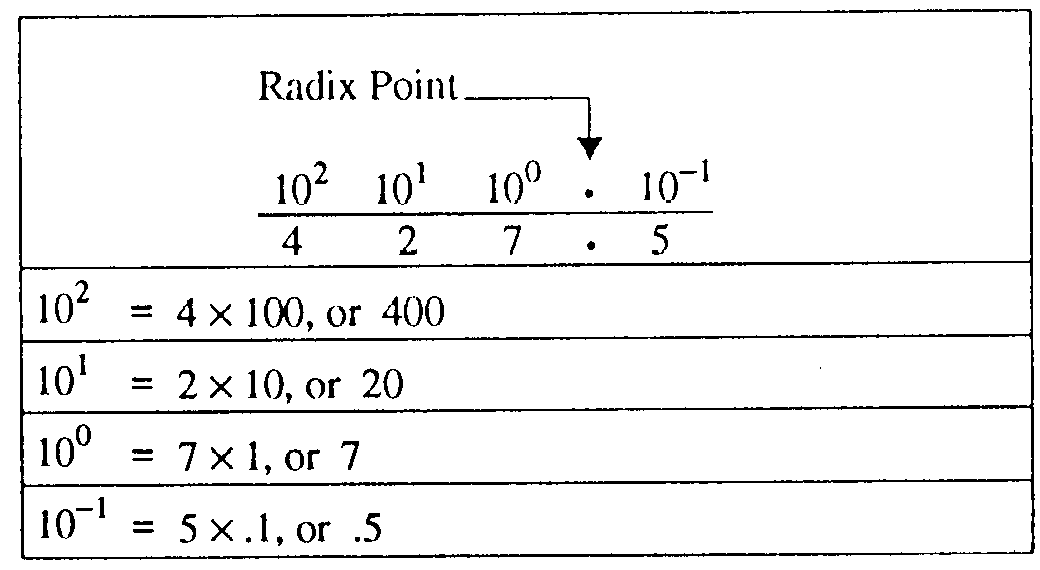
Positional notation is a system where the value of a number is defined not only by the symbol but by the symbol’s position. Let’s examine the decimal (base 10) value of 427.5. You know from experience that this value is four hundred twenty-seven and one-half. Now examine the position of each number:
If 427.5 is the quantity you wish to express, then each number must be in the position shown. If you exchange the positions of the 2 and the 7, then you change the value.
1-4
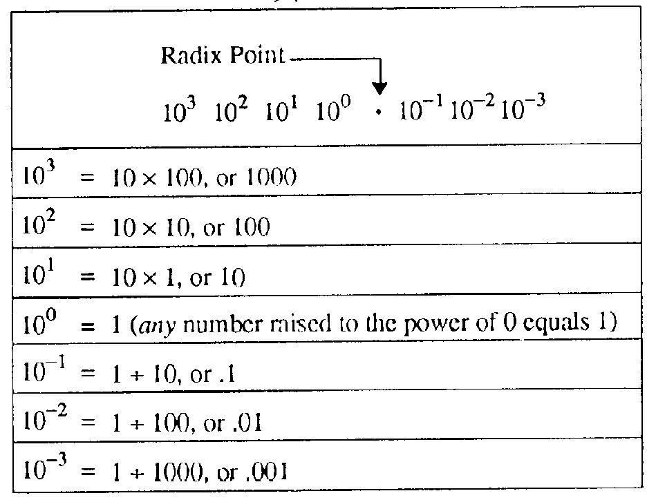
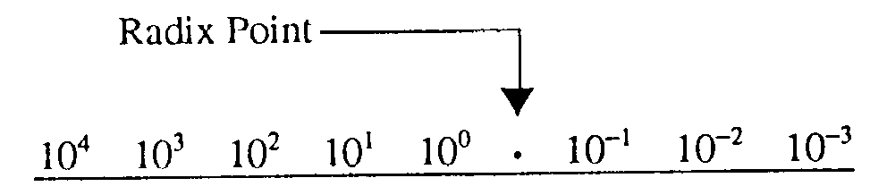
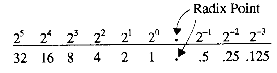
Each position in the positional notation system represents a power of the base, or radix. A POWER is the number of times a base is multiplied by itself. The power is written above and to the right of the base and is called an EXPONENT. Examine the following base 10 line graph:
Now let’s look at the value of the base 10 number 427.5 with the positional notation line graph:
You can see that the power of the base is multiplied by the number in that position to determine the value for that position.
The following graph illustrates the progression of powers of 10:
1-5
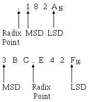
All numbers to the left of the decimal point are whole numbers, and all numbers to the right of the decimal point are fractional numbers. A whole number is a symbol that represents one, or more, complete objects, such as one apple or $5. A fractional number is a symbol that represents a portion of an object, such as half of an apple (.5 apples) or a quarter of a dollar ($0.25). A mixed number represents one, or more, complete objects, and some portion of an object, such as one and a half apples (1.5 apples). When you use any base other than the decimal system, the division between whole numbers and fractional numbers is referred to as the RADIX POINT. The decimal point is actually the radix point of the decimal system, but the term radix point is normally not used with the base 10 number system.
Just as important as positional notation is the use of the zero. The placement of the zero in a number can have quite an effect on the value being represented. Sometimes a position in a number does not have a value between 1 and 9. Consider how this would affect your next paycheck. If you were expecting a check for $605.47, you wouldn’t want it to be $65.47. Leaving out the zero in this case means a difference of $540.00. In the number 605.47, the zero indicates that there are no tens. If you place this value on a bar graph, you will see that there are no multiples of 101.
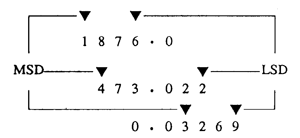
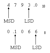
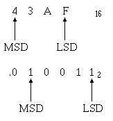
Most Significant Digit and Least Significant Digit (MSD and LSD) Other important factors of number systems that you should recognize are the MOST SIGNIFICANT
DIGIT (MSD) and the LEAST SIGNIFICANT DIGIT (LSD). The MSD in a number is the digit that has the greatest effect on that number.
The LSD in a number is the digit that has the least effect on that number.
Look at the following examples:
1-6
You can easily see that a change in the MSD will increase or decrease the value of the number the greatest amount. Changes in the LSD will have the smallest effect on the value. The nonzero digit of a
number that is the farthest LEFT is the MSD, and the nonzero digit farthest RIGHT is the LSD, as in the following example:
In a whole number the LSD will always be the digit immediately to the left of the radix point.
Q1. What term describes a single object? Q2. A symbol that represents one or more objects is called a _________. Q3. The symbols 0, 1, 2, and 3 through 9 are what type of numerals? Q4. What does the base, or radix, of a number system tell you about the system? Q5. How would you write one hundred seventy-three base 10? Q6. What power of 10 is equal to 1,000? 100? 10? 1? Q7. The decimal point of the base 10 number system is also known as the _________.
1-7
Q8. What is the MSD and LSD of the following numbers (a) 420. (b) 1045.06 (c) 0.0024 (d) 247.0001
Carry and Borrow Principles
Soon after you learned how to count, you were taught how to add and subtract. At that time, you learned some concepts that you use almost everyday. Those concepts will be reviewed using the decimal system. They will also be applied to the other number systems you will study.
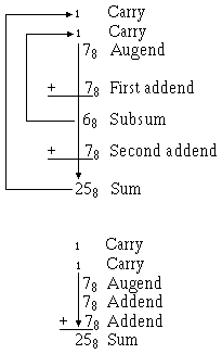
ADDITION¾ Addition is a form of counting in which one quantity is added to another. The following definitions identify the basic terms of addition:
AUGEND¾ The quantity to which an addend is added
ADDEND¾ A number to be added to a preceding number
SUM ¾ The result of an addition (the sum of 5 and 7 is 12) CARRY ¾ A carry is produced when the sum of two or more digits in a vertical column equals or exceeds the base of the number system in use
How do we handle the carry; that is, the two-digit number generated when a carry is produced? The lower order digit becomes the sum of the column being added; the higher order digit (the carry) is added to the next higher order column. For example, let’s add 15 and 7 in the decimal system:
Starting with the first column, we find the sum of 5 and 7 is 12. The 2 becomes the sum of the lower order column and the 1 (the carry) is added to the upper order column. The sum of the upper order column is 2. The sum of 15 and 7 is, therefore, 22.
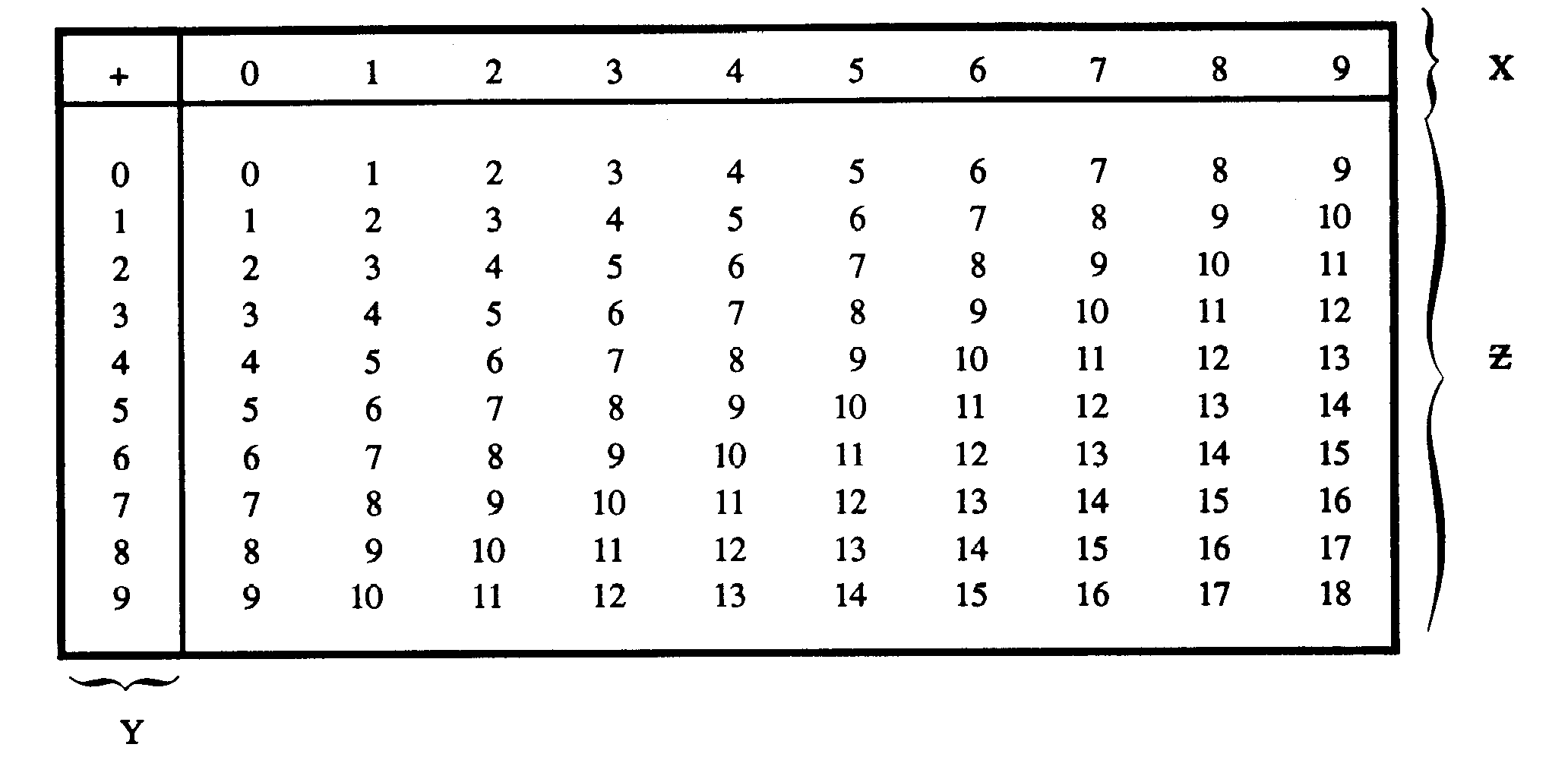
The rules for addition are basically the same regardless of the number system being used. Each number system, because it has a different number of digits, will have a unique digit addition table. These addition tables will be described during the discussion of the adding process for each number system.
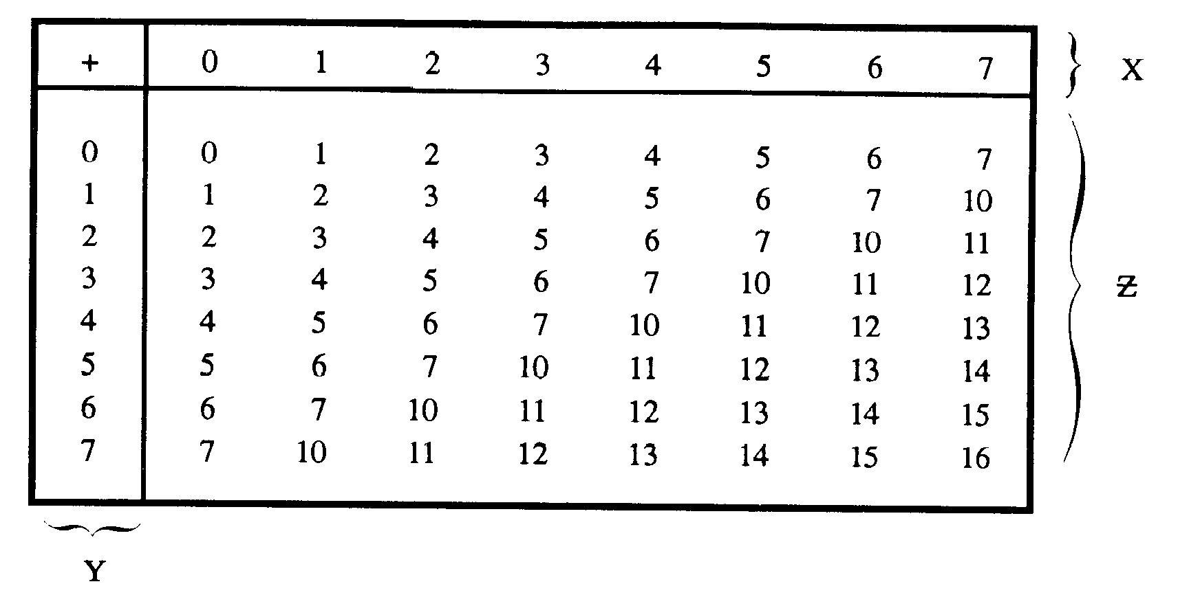
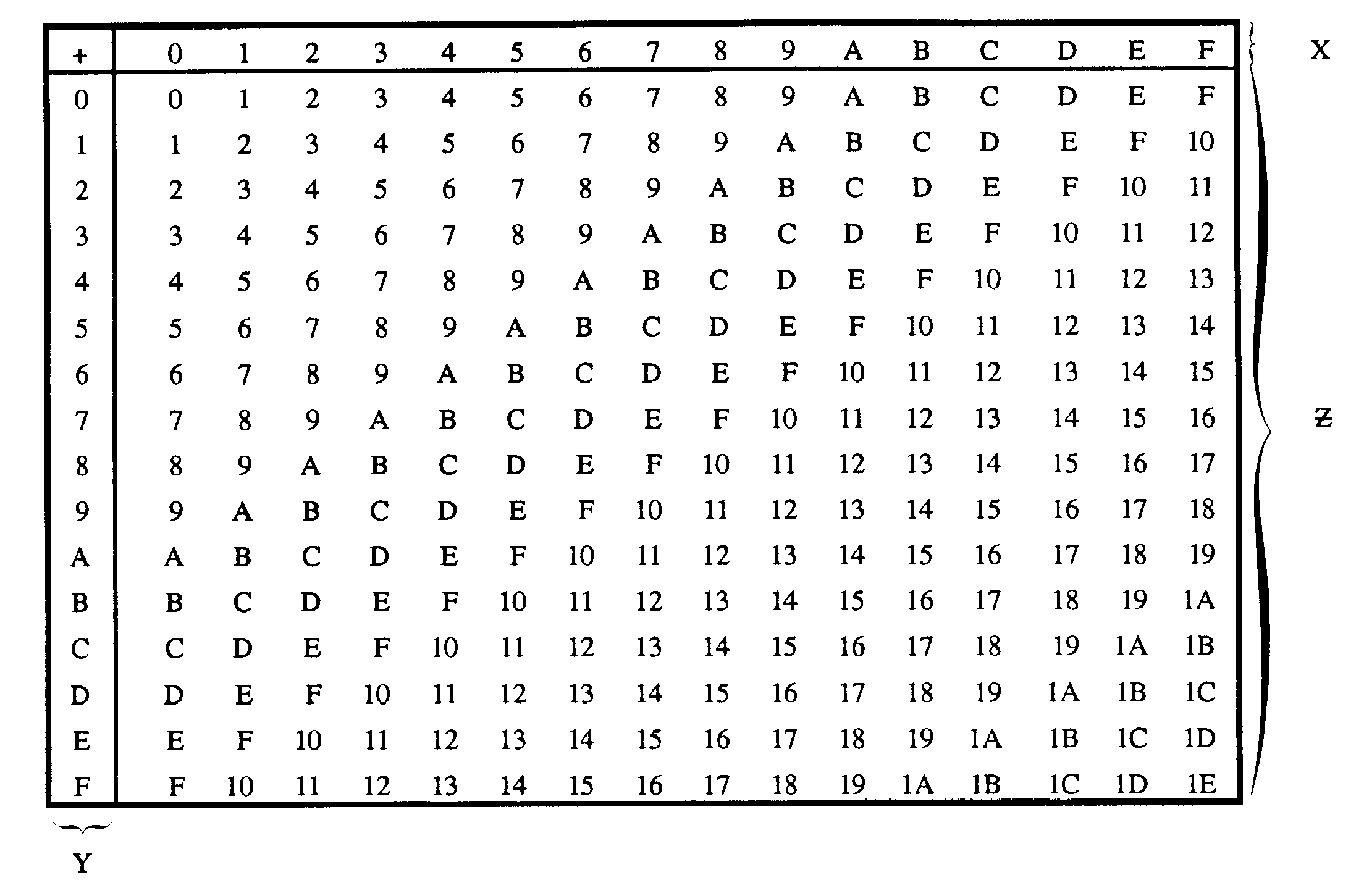
A decimal addition table is shown in table 1-1. The numbers in row X and column Y may represent either the addend or the augend. If the numbers in X represent the augend, then the numbers in Y must represent the addend and vice versa. The sum of X + Y is located at the point in array Z where the selected X row and Y column intersect.
1-8
Table 1-1. —Decimal Addition Table
To add 5 and 7 using the table, first locate one number in the X row and the other in the Y column. The point in field Z where the row and column intersect is the sum. In this case the sum is 12.
SUBTRACTION.¾ The following definitions identify the basic terms you will need to know to understand subtraction operations:
• SUBTRACT¾ To take away, as a part from the whole or one number from another
• MINUEND¾ The number from which another number is to be subtracted
• SUBTRAHEND¾ The quantity to be subtracted
• REMAINDER, or DIFFERENCE ¾ That which is left after subtraction
• BORROW ¾ To transfer a digit (equal to the base number) from the next higher order column for the purpose of subtraction.
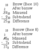
Use the rules of subtraction and subtract 8 from 25. The form of this problem is probably familiar to you:
It requires the use of the borrow; that is, you cannot subtract 8 from 5 and have a positive difference. You must borrow a 1, which is really one group of 10. Then, one group of 10 plus five groups of 1 equal 15, and 15 minus 8 leaves a difference of 7. The 2 was reduced by 1 by the borrow; and since nothing is to be subtracted from it, it is brought down to the difference.
Since the process of subtraction is the opposite of addition, the addition table 1-1 may be used to illustrate subtraction facts for any number system we may discuss.
1-9
In addition,
X + Y = Z
In subtraction, the reverse is true; that is,
Z – Y = X
OR
Z – X = Y
Thus, in subtraction the minuend is always found in array Z and the subtrahend in either row X or column Y. If the subtrahend is in row X, then the remainder will be in column Y. Conversely, if the subtrahend is in column Y, then the difference will be in row X. For example, to subtract 8 from 15, find 8 in either the X row or Y column. Find where this row or column intersects with a value of 15 for Z; then move to the remaining row or column to find the difference.
THE BINARY NUMBER SYSTEM
The simplest possible number system is the BINARY, or base 2, system. You will be able to use the information just covered about the decimal system to easily relate the same terms to the binary system. Unit and Number
The base, or radix¾ you should remember from our decimal section ¾ is the number of symbols used in the number system. Since this is the base 2 system, only two symbols, 0 and 1, are used. The base is indicated by a subscript, as shown in the following example:
12
When you are working with the decimal system, you normally don't use the subscript. Now that you will be working with number systems other than the decimal system, it is important that you use the subscript so that you are sure of the system being referred to. Consider the following two numbers:
11 11
With no subscript you would assume both values were the same. If you add subscripts to indicate their base system, as shown below, then their values are quite different:
1110 112
The base ten number 1110 is eleven, but the base two number 112 is only equal to three in base ten. There will be occasions when more than one number system will be discussed at the same time, so you MUST use the proper Subscript.
Positional Notation
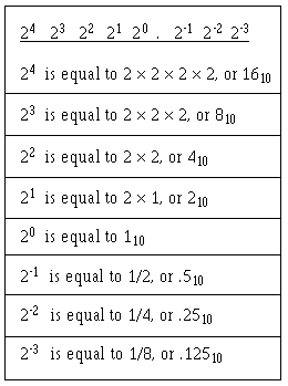
As in the decimal number system, the principle of positional notation applies to the binary number system. You should recall that the decimal system uses powers of 10 to determine the value of a position. The binary system uses powers of 2 to determine the value of a position. A bar graph showing the positions and the powers of the base is shown below:
1-10
All numbers or values to the left of the radix point are whole numbers, and all numbers to the right of the radix point are fractional numbers.
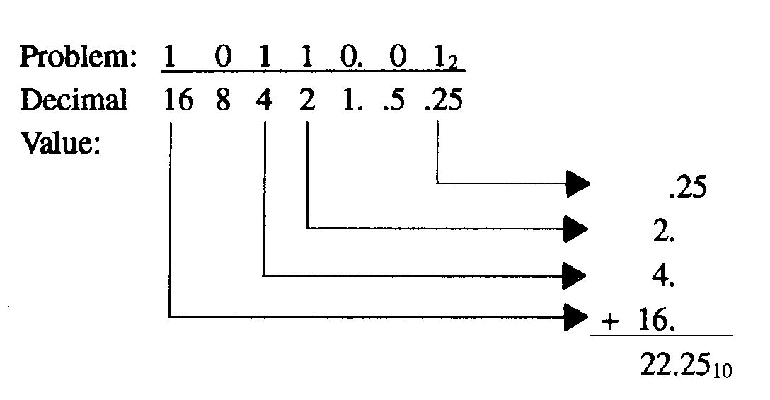
Let’s look at the binary number 101.1 on a bar graph:
Working from the radix point to the right and left, you can determine the decimal equivalent:
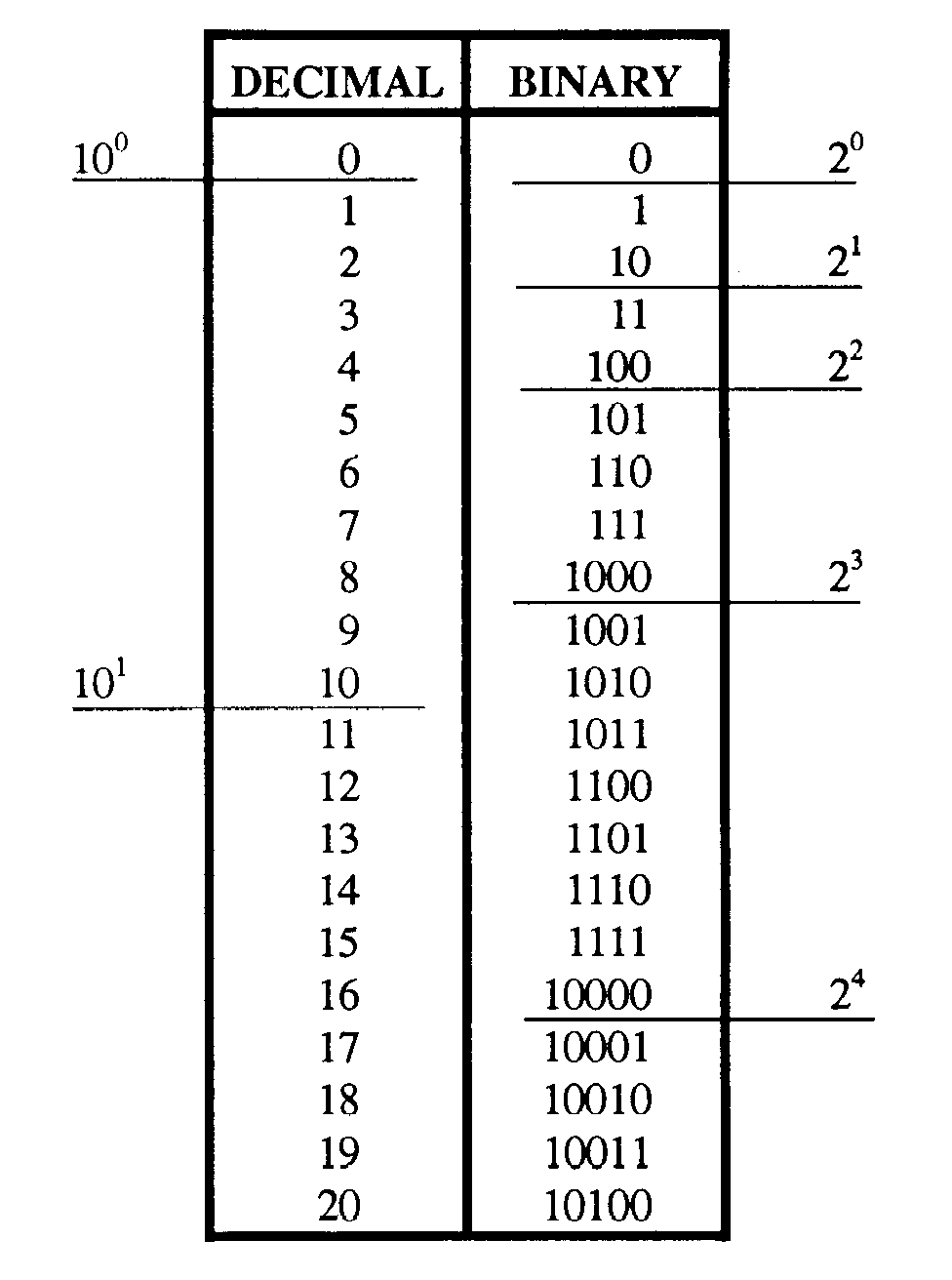
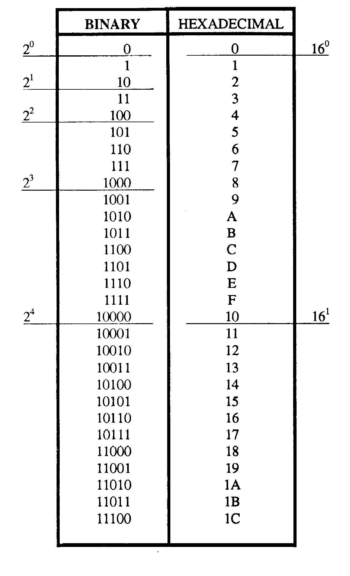
Table 1-2 provides a comparison of decimal and binary numbers. Notice that each time the total number of binary symbol positions increase, the binary number indicates the next higher power of 2. By this example, you can also see that more symbol positions are needed in the binary system to represent the equivalent value in the decimal system.
1-11
Table 1-2. —Decimal and Binary Comparison
MSD and LSD
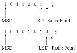
When you’re determining the MSD and LSD for binary numbers, use the same guidelines you used with the decimal system. As you read from left to right, the first nonzero digit you encounter is the MSD, and the last nonzero digit is the LSD.
If the number is a whole number, then the first digit to the left of the radix point is the LSD.

Figure 1-1. —Binary Example
1-12
Here, as in the decimal system, the MSD is the digit that will have the most effect on the number; the LSD is the digit that will have the least effect on the number.
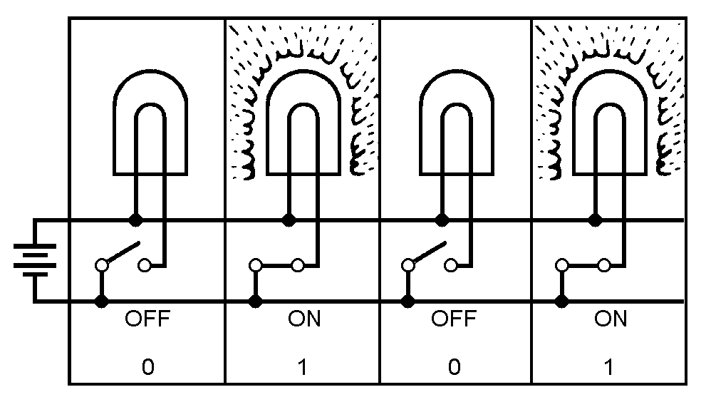
The two numerals of the binary system (1 and 0) can easily be represented by many electrical or electronic devices. For example, 12 may be indicated when a device is active (on), and 02 may be indicated when a device is nonactive (off).
Look at the preceding figure. It illustrates a very simple binary counting device. Notice that 12 is indicated by a lighted lamp and 02 is indicated by an unlighted lamp. The reverse will work equally well. The unlighted state of the lamp can be used to represent a binary 1 condition, and the lighted state can represent the binary 0 condition. Both methods are used in digital computer applications. Many other devices are used to represent binary conditions. They include switches, relays, diodes, transistors, and integrated circuits (ICs). Addition of Binary Numbers
Addition of binary numbers is basically the same as addition of decimal numbers. Each system has an augend, an addend, a sum, and carries. The following example will refresh your memory:
Since only two symbols, 0 and 1, are used with the binary system, only four combinations of addition are possible.
0 + 0
1 + 0
0 + 1
1 + 1
1-13
The sum of each of the first three combinations is obvious:
0 + 0 = 02
0 + 1 = 12
1 + 0 = 12
The fourth combination presents a different situation. The sum of 1 and 1 in any other number system is 2, but the numeral 2 does not exist in the binary system. Therefore, the sum of 12 and 12 is 102 (spoken as one zero base two), which is equal to 210.
Study the following examples using the four combinations mentioned above:
When a carry is produced, it is noted in the column of the next higher value or in the column immediately to the left of the one that produced the carry.
Example: Add 10112 and 11012.
Solution: Write out the problem as shown:
As we noted previously, the sum of 1 and 1 is 2, which cannot be expressed as a single digit in the binary system. Therefore, the sum of 1 and 1 produces a carry:
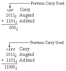
1-14
The following steps, with the carry indicated, show the completion of the addition:
When the carry is added, it is marked through to prevent adding it twice.
In the final step the remaining carry is brought down to the sum.
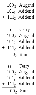
In the following example you will see that more than one carry may be produced by a single column. This is something that does not occur in the decimal system.
Example: Add 12, 12, 12, and 12
The sum of the augend and the first addend is 0 with a carry. The sum of the second and third addends is also 0 with a carry. At this point the solution resembles the following example:
The sum of the carries is 0 with a carry, so the sum of the problem is as follows:
1-15
The same situation occurs in the following example:
Add 1002, 1012, and 1112
As in the previous example, the sum of the four 1s is 0 with two carries, and the sum of the two carries is 0 with one carry. The final solution will look like this:
In the addition of binary numbers, you should remember the following binary addition rules:
1-16
Now practice what you’ve learned by solving the following problems:
Q9.
Q10.
Q11.
Q12.
Q13.
1-17
Q14.
Subtraction of Binary Numbers
Now that you are familiar with the addition of binary numbers, subtraction will be easy. The following are the four rules that you must observe when subtracting:
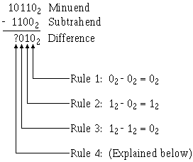
Rule 1: 02 – 02 = 02
Rule 2: 12 – 02 = 12
Rule 3: 02 – 12 = 12
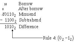
Rule 4: 12 – 12 = 12 with a borrow
The following example (101102 - 11002) demonstrates the four rules of binary subtraction:
Rule 4 presents a different situation because you cannot subtract 1 from 0. Since you cannot subtract 1 from 0 and have a positive difference, you must borrow the 1 from the next higher order column of the minuend. The borrow may be indicated as shown below:
1-18
Now observe the following method of borrowing across more than one column in the example, 10002 - 12:
Let’s practice some subtraction by solving the following problems:
Q15. Subtract:
Q16. Subtract:
Q17. Subtract:
1-19
Q18. Subtract:
Q19. Subtract:
Q20. Subtract:
Complementary Subtraction
If you do any work with computers, you will soon find out that most digital systems cannot subtract ¾ they can only add. You are going to need a method of adding that gives the results of subtraction. Does that sound confusing? Really, it is quite simple. A COMPLEMENT is used for our subtractions. A complement is something used to complete something else.
In most number systems you will find two types of complements. The first is the amount necessary to complete a number up to the highest number in the number system. In the decimal system, this would be the difference between a given number and all 9s. This is called the nines complement or the radix-1 or R’s-1 complement. As an example, the nines complement of 254 is 999 minus 254, or 745.
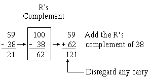
The second type of complement is the difference between a number and the next higher power of the number base. As an example, the next higher power of 10 above 999 is 1,000. The difference between 1,000 and 254 is 746. This is called the tens complement in the decimal number system. It is also called the radix or R’s complement. We will use complements to subtract. Let’s look at the magic of this process. There are three important points we should mention before we start: (1) Never complement the minuend in a problem, (2) always disregard any carry beyond the number of positions of the largest of the original numbers, and (3) add the R’s complement of the original subtrahend to the original minuend. This will have the same effect as subtracting the original number. Let’s look at a base ten example in which we subtract 38 from 59:
1-20
Now let’s look at the number system that most computers use, the binary system. Just as the decimal system, had the nines (R’s-1) and tens (R’s) complement, the binary system has two types of complement methods. These two types are the ones (R’s-1) complement and the twos (R’s) complement. The binary system R’s-1 complement is the difference between the binary number and all 1s. The R’s complement is the difference between the binary number and the next higher power of 2.
Let’s look at a quick and easy way to form the R’s-1 complement. To do this, change each 1 in the original number to 0 and each 0 in the original number to 1 as has been done in the example below.
10110112
1001002 R’s-1 complement
There are two methods of achieving the R’s complement. In the first method we perform the R’s-1 complement and then add 1. This is much easier than subtracting the original number from the next higher power of 2. If you had subtracted, you would have had to borrow.
Saying it another way, to reach the R’s complement of any binary number, change all 1s to 0s and all 0s to 1s, and then add 1.
As an example let’s determine the R’s complement of 101011012:
The second method of obtaining the R’s complement will be demonstrated on the binary number 001011011002.
Step 1—Start with the LSD, working to the MSD, writing the digits as they are up to and including the first one.
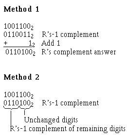
1-21
Step 2—Now R's-1 complement the remaining digits:
Now let's R's complement the same number using both methods:
Now let's do some subtracting by using the R's complement method. We will go through the subtraction of 310 from 910 (00112from 10012):
Step 1¾ Leave the minuend alone:
10012 remains 10012
Step 2—Using either method, R's complement the subtrahend:
11012 R's complement of subtrahend
Step 3¾ Add the R's complement found in step 2 to the minuend of the original problem:
1-22
Step 4—Remember to discard any carry beyond the size of the original number. Our original problem had four digits, so we discard the carry that expanded the difference to five digits. This carry we disregard is significant to the computer. It indicates that the difference is positive. Because we have a carry, we can read the difference directly without any further computations. Let's check our answer:
If we do not have a carry, it indicates the difference is a negative number. In that case, the difference must be R's complemented to produce the correct answer.
Let's look at an example that will explain this for you.
Subtract 910 from 510 (10012 from 01012):
Step 1—Leave the minuend alone:
01012 remains 01012
Step 2—R's complement the subtrahend:
01112 R's complement of subtrahend
Step 3—Add the R's complement found in step 2 to the minuend of the original problem:
Step 4—We do not have a carry; and this tells us, and any computer, that our difference (answer) is negative. With no carry, we must R's complement the difference in step 3. We will then have arrived at the answer (difference) to our original problem. Let's do this R's complement step and then check our answer:
01002 R's complement of difference in step 3
Remember, we had no carry in step 3. That showed us our answer was going to be negative. Make sure you indicate the difference is negative. Let's check the answer to our problem:
1-23
Try solving a few subtraction problems by using the complement method:
Q21. Subtract:
Q22. Subtract:
Q23. Subtract:
OCTAL NUMBER SYSTEM
The octal, or base 8, number system is a common system used with computers. Because of its relationship with the binary system, it is useful in programming some types of computers.
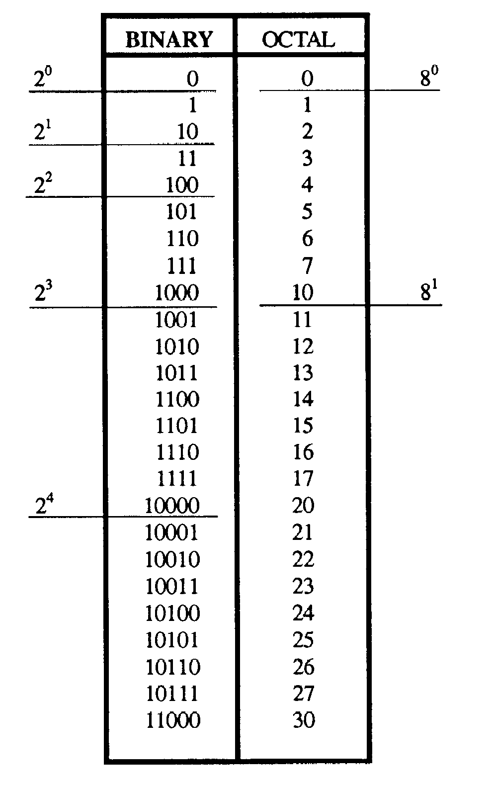
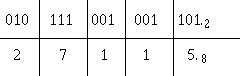
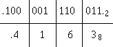
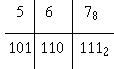
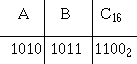
Look closely at the comparison of binary and octal number systems in table 1-3. You can see that one octal digit is the equivalent value of three binary digits. The following examples of the conversion of octal 2258 to binary and back again further illustrate this comparison:
1-24
Table 1-3. —Binary and Octal Comparison
Unit and Number
The terms that you learned in the decimal and binary sections are also used with the octal system.
The unit remains a single object, and the number is still a symbol used to represent one or more units.
Base (Radix) As with the other systems, the radix, or base, is the number of symbols used in the system. The octal
system uses eight symbols ¾ 0 through 7. The base, or radix, is indicated by the subscript 8.
Positional Notation
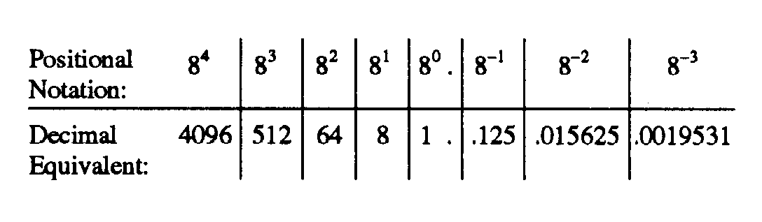
The octal number system is a positional notation number system. Just as the decimal system uses powers of 10 and the binary system uses powers of 2, the octal system uses power of 8 to determine the value of a number’s position. The following bar graph shows the positions and the power of the base:
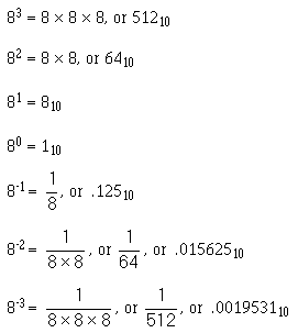
83 82 81 80 ���-1 8-2 8-3
1-25
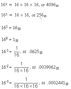
Remember, that the power, or exponent, indicates the number of times the base is multiplied by itself. The value of this multiplication is expressed in base 10 as shown below:
All numbers to the left of the radix point are whole numbers, and those to the right are fractional numbers.
MSD and LSD
When determining the most and least significant digits in an octal number, use the same rules that you used with the other number systems. The digit farthest to the left of the radix point is the MSD, and the one farthest right of the radix point is the LSD.
Example:
If the number is a whole number, the MSD is the nonzero digit farthest to the left of the radix point and the LSD is the digit immediately to the left of the radix point. Conversely, if the number is a fraction only, the nonzero digit closest to the radix point is the MSD and the LSD is the nonzero digit farthest to the right of the radix point.
Addition of Octal Numbers
The addition of octal numbers is not difficult provided you remember that anytime the sum of two digits exceeds 7, a carry is produced. Compare the two examples shown below:
1-26
The octal addition table in table 1-4 will be of benefit to you until you are accustomed to adding octal numbers. To use the table, simply follow the directions used in this example:
Add: 68 and 58
Table 1-4. —Octal Addition Table
Locate the 6 in the X column of the figure. Next locate the 5 in the Y column. The point in area Z where these two columns intersect is the sum. Therefore,
If you use the concepts of addition you have already learned, you are ready to add octal numbers.
Work through the solutions to the following problems:
1-27
As was mentioned earlier in this section, each time the sum of a column of numbers exceeds 7, a carry is produced. More than one carry may be produced if there are three or more numbers to be added, as in this example:
The sum of the augend and the first addend is 68 with a carry. The sum of 68 and the second addend is 58 with a carry. You should write down the 58 and add the two carries and bring them down to the sum, as shown below:
Now let’s try some practice problems:
Q24. Add:
Q25. Add:
1-28
Q26. Add:
Q27. Add:
Q28. Add
Q29. Add:
Subtraction of Octal Numbers
The subtraction of octal numbers follows the same rules as the subtraction of numbers in any other number system. The only variation is in the quantity of the borrow. In the decimal system, you had to borrow a group of 1010. In the binary system, you borrowed a group of 210. In the octal system you will borrow a group of 810.
Consider the subtraction of 1 from 10 in decimal, binary, and octal number systems:
1-29
In each example, you cannot subtract 1 from 0 and have a positive difference. You must use a borrow from the next column of numbers. Let’s examine the above problems and show the borrow as a decimal quantity for clarity:
When you use the borrow, the column you borrow from is reduced by 1, and the amount of the borrow is added to the column of the minuend being subtracted. The following examples show this procedure:
In the octal example 78 cannot be subtracted from 68, so you must borrow from the 4. Reduce the 4 by 1 and add 108 (the borrow) to the 68 in the minuend. By subtracting 78 from 168, you get a difference of 78. Write this number in the difference line and bring down the 3. You may need to refer to table 1-4, the octal addition table, until you are familiar with octal numbers. To use the table for subtraction, follow these directions. Locate the subtrahend in column Y. Now find where this line intersects with the minuend in area Z. The remainder, or difference, will be in row X directly above this point.
Do the following problems to practice your octal subtraction:
Q30. Subtract:
Q31. Subtract:
1-30
Q32. Subtract:
Q33. Subtract:
Q34. Subtract:
Q35. Subtract:
Check your answers by adding the subtrahend and difference for each problem.
HEXADECIMAL (HEX) NUMBER SYSTEM The hex number system is a more complex system in use with computers. The name is derived from
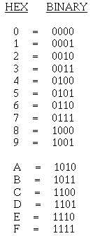
the fact the system uses 16 symbols. It is beneficial in computer programming because of its relationship to the binary system. Since 16 in the decimal system is the fourth power of 2 (or 24); one hex digit has a value equal to four binary digits. Table 1-5 shows the relationship between the two systems.
1-31
Table 1-5. —Binary and Hexadecimal Comparison
Unit and Number
As in each of the previous number systems, a unit stands for a single object. A number in the hex system is the symbol used to represent a unit or quantity. The Arabic numerals
0 through 9 are used along with the first six letters of the alphabet. You have probably used letters in math problems to represent unknown quantities, but in the hex system A, B, C, D, E, and F, each have a definite value as shown below:
1-32
Base (Radix) The base, or radix, of this system is 16, which represents the number of symbols used in the system.
A quantity expressed in hex will be annotated by the subscript 16, as shown below:
A3EF16
Positional Notation
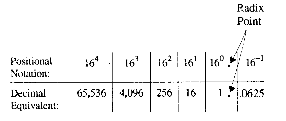
Like the binary, octal, and decimal systems, the hex system is a positional notation system. Powers of 16 are used for the positional values of a number. The following bar graph shows the positions:
163 162 161 160 ���-1 16-2 16-3
Multiplying the base times itself the number of times indicated by the exponent will show the equivalent decimal value:
1-33
You can see from the positional values that usually fewer symbol positions are required to express a number in hex than in decimal. The following example shows this comparison:
62516 is equal to 157310
MSD and LSD
The most significant and least significant digits will be determined in the same manner as the other number systems. The following examples show the MSD and LSD of whole, fractional, and mixed hex numbers:
Addition of Hex Numbers
The addition of hex numbers may seem intimidating at first glance, but it is no different than addition in any other number system. The same rules apply. Certain combinations of symbols produce a carry while others do not. Some numerals combine to produce a sum represented by a letter. After a little practice you will be as confident adding hex numbers as you are adding decimal numbers.
Study the hex addition table in table 1-6. Using the table, add 7 and 7. Locate the number 7 in both columns X and Y. The point in area Z where these two columns intersect is the sum; in this case 7 + 7 = E. As long as the sum of two numbers is 1510 or less, only one symbol is used for the sum. A carry will be produced when the sum of two numbers is 1610 or greater, as in the following examples:
1-34
Table 1-6. —Hexadecimal Addition Table
Use the addition table and follow the solution of the following problems:
In this example each column is straight addition with no carry.
Now add the addend (78416) and the sum (BDA16) of the previous problem:
Here the sum of 4 and A is E. Adding 8 and D is 1516; write down 5 and carry a 1. Add the first carry to the 7 in the next column and add the sum, 8, to B. The result is 1316; write down 3 and carry a 1. Since only the last carry is left to add, bring it down to complete the problem.
Now observe the procedures for a more complex addition problem. You may find it easier to add the Arabic numerals in each column first:
1-35
The sum of 4, E, 1, and 3 in the first column is 1616. Write down the 6 and the carry. In the second column, 1, 1, 9, and 7 equals 1216. Write the carry over the next column. Add B and 2 ¾ the sum is D. Write this in the sum line. Now add the final column, 1, 1, 5, and C. The sum is 1316. Write down the carry; then add 3 and B ¾ the sum is E. Write down the E and bring down the final carry to complete the problem.
Now solve the following addition problems:
Q36. Add:
Q37. Add:
Q38. Add:
Q39. Add:
Q40. Add:
1-36
Q41. Add:
Subtraction of Hex Numbers
The subtraction of hex numbers looks more difficult than it really is. In the preceding sections you learned all the rules for subtraction. Now you need only to apply those rules to a new number system. The symbols may be different and the amount of the borrow is different, but the rules remain the same.
Use the hex addition table (table 1-6) to follow the solution of the following problems:
Working from left to right, first locate the subtrahend (2) in column Y. Follow this line across area Z until you reach C. The difference is located in column X directly above the C ¾ in this case A. Use this same procedure to reach the solution:
Now examine the following solutions:
In the previous example, when F was subtracted from 1E, a borrow was used. Since you cannot subtract F from E and have a positive difference, a borrow of 1016 was taken from the next higher value column. The borrow was added to E, and the higher value column was reduced by 1.
The following example shows the use of the borrow in a more difficult problem:
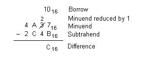
1-37
In this first step, B cannot be subtracted from 7, so you take a borrow of 1016 from the next higher value column. Add the borrow to the 7 in the minuend; then subtract (1716 minus B16 equals C16). Reduce the number from which the borrow was taken (3) by 1.
To subtract 416 from 216 also requires a borrow, as shown below:
Borrow 1016 from the A and reduce the minuend by 1. Add the borrow to the 2 and subtract 416 from 1216. The difference is E.
When solved the problem looks like this:
Remember that the borrow is 1016 not 1010.
There may be times when you need to borrow from a column that has a 0 in the minuend. In that case, you borrow from the next highest value column, which will provide you with a value in the 0 column that you can borrow from.
To subtract A from 7, you must borrow. To borrow you must first borrow from the 2. The 0 becomes 1016, which can give up a borrow. Reduce the 1016 by 1 to provide a borrow for the 7. Reducing 1016 by 1 equals F. Subtracting A16 from 1716 gives you D16. Bring down the 1 and F for a difference of 1FD16.
Now let’s practice what we’ve learned by solving the following hex subtraction problems:

1-38
Q42. Subtract:
Q43. Subtract:
Q44. Subtract:
Q45. Subtract:
Q46. Subtract:
Q47. Subtract:
CONVERSION OF BASES
We mentioned in the introduction to this chapter that digital computers operate on electrical pulses. These pulses or the absence of, are easily represented by binary numbers. A pulse can represent a binary 1, and the lack of a pulse can represent a binary 0 or vice versa.
1-39
The sections of this chapter that discussed octal and hex numbers both mentioned that their number systems were beneficial to programmers. You will see later in this section that octal and hex numbers are easily converted to binary numbers and vice versa..
If you are going to work with computers, there will be many times when it will be necessary to convert decimal numbers to binary, octal, and hex numbers. You will also have to be able to convert binary, octal, and hex numbers to decimal numbers. Converting each number system to each of the others will be explained. This will prepare you for converting from any base to any other base when needed.
DECIMAL CONVERSION
Some computer systems have the capability to convert decimal numbers to binary numbers. They do this by using additional circuitry. Many of these systems require that the decimal numbers be converted to another form before entry.
Decimal to Binary
Conversion of a decimal number to any other base is accomplished by dividing the decimal number by the radix of the system you are converting to. The following definitions identify the basic terms used in division:
• DIVIDEND¾ The number to be divided
• DIVISOR¾ The number by which a dividend is divided
• QUOTIENT ¾ The number resulting from the division of one number by another • REMAINDER¾ The final undivided part after division that is less or of a lower degree than the
divisor
To convert a base 10 whole number to its binary equivalent, first set up the problem for division:
Step 1—Divide the base 10 number by the radix (2) of the binary system and extract the remainder (this becomes the binary number's LSD).
Step 2—Continue the division by dividing the quotient of step 1 by the radix (2 �����
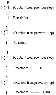
1-40
Step 3—Continue dividing quotients by the radix until the quotient becomes smaller that the divisor; then do one more division. The remainder is our MSD.
The remainder in step 1 is our LSD. Now rewrite the solution, and you will see that 510 equals 1012. Now follow the conversion of 2310 to binary:
Step 1—Set up the problem for division:
Step 2—Divide the number and extract the remainder:
1-41
Step 3—Rewrite the solution from MSD to LSD:
101112
No matter how large the decimal number may be, we use the same procedure. Let's try the problem below. It has a larger dividend:
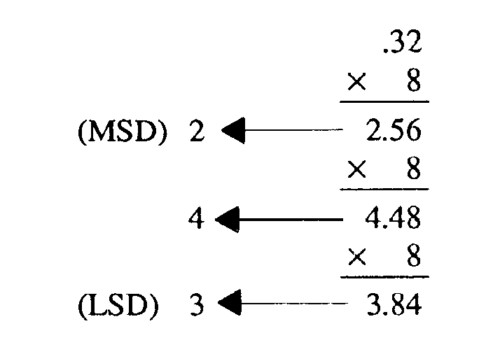
We can convert fractional decimal numbers by multiplying the fraction by the radix and extracting the portion of the product to the left of the radix point. Continue to multiply the fractional portion of the previous product until the desired degree of accuracy is attained.
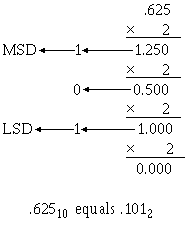
1-42
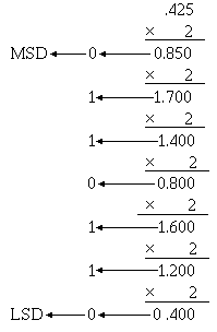
Let’s go through this process and convert 0.2510 to its binary equivalent:
The first figure to the left of the radix point is the MSD, and the last figure of the computation is the LSD. Rewrite the solution from MSD to LSD preceded by the radix point as shown:
.012
Now try converting .62510 to binary:
As we mentioned before, you should continue the operations until you reach the desired accuracy. For example, convert .42510 to five places in the binary system:
1-43
Although the multiplication was carried out for seven places, you would only use what is required. Write out the solution as shown:
.011012
To convert a mixed number such as 37.62510 to binary, split the number into its whole and fractional components and solve each one separately. In this problem carry the fractional part to four places. When the conversion of each is completed, recombine it with the radix point as shown below:
3710 = 1001012
.62510 = .10102
37.62510 = 100101.10102
Convert the following decimal numbers to binary:
Q48. 7210. Q49. 9710. Q50. 24310. Q51. 0.87510 (four places). Q52. 0.3310 (four places). Q53. 17.4210 (five places)
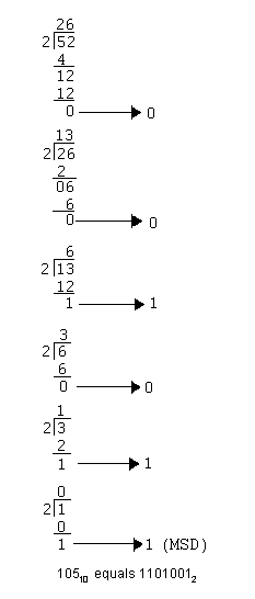
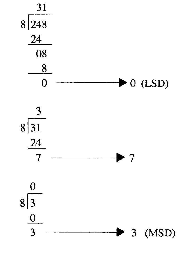
Decimal to Octal
The conversion of a decimal number to its base 8 equivalent is done by the repeated division method. You simply divide the base 10 number by 8 and extract the remainders. The first remainder will be the LSD, and the last remainder will be the MSD.
Look at the following example. To convert 1510 to octal, set up the problem for division:
Since 8 goes into 15 one time with a 7 remainder, 7 then is the LSD. Next divide 8 into the quotient (1). The result is a 0 quotient with a 1 remainder. The 1 is the MSD:
1-44
Now write out the number from MSD to LSD as shown:
178
The same process is used regardless of the size of the decimal number. Naturally, more divisions are needed for larger numbers, as in the following example:
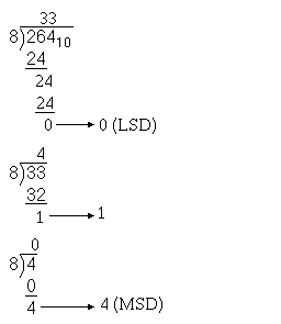
Convert 26410 to octal:
By rewriting the solution, you find that the octal equivalent of 26410 is as follows:
4108
To convert a decimal fraction to octal, multiply the fraction by 8. Extract everything that appears to the left of the radix point. The first number extracted will be the MSD and will follow the radix point. The last number extracted will be the LSD.
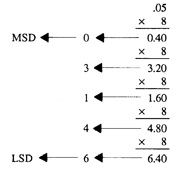
Convert 0.0510 to octal:
1-45
Write the solution from MSD to LSD:
.031468
You can carry the conversion out to as many places as needed, but usually four or five places are enough.
To convert a mixed decimal number to its octal equivalent, split the number into whole and fractional portions and solve as shown below:
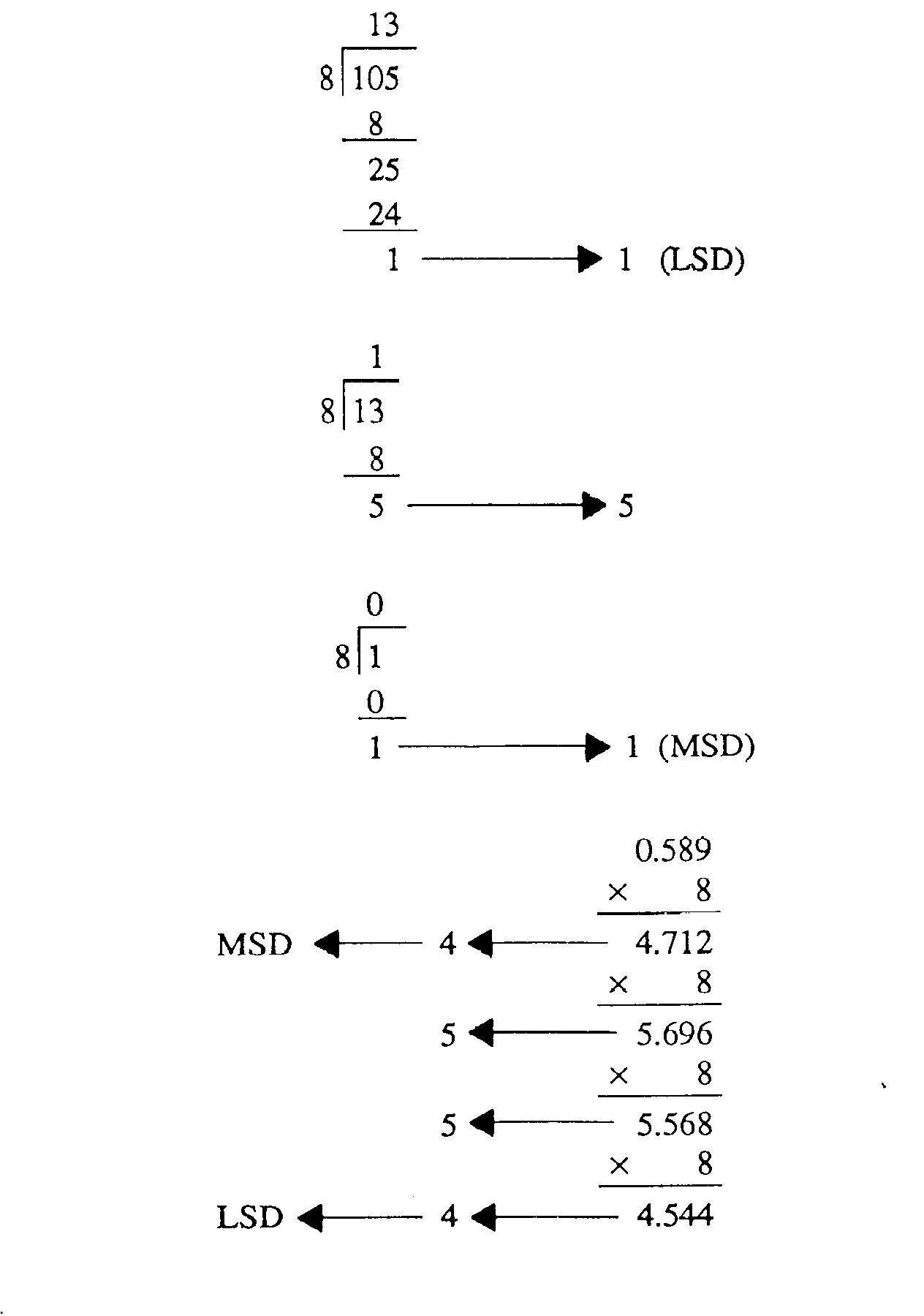
Convert 105.58910 to octal:
Combine the portions into a mixed number:
151.45548
Convert the following decimal numbers to octal:
Q54. 710
1-46
Q55. 4310 Q56. 49910 Q57. 0.95110 (four places). Q58. 0.00410 (five places). Q59. 252.1710 (three places).
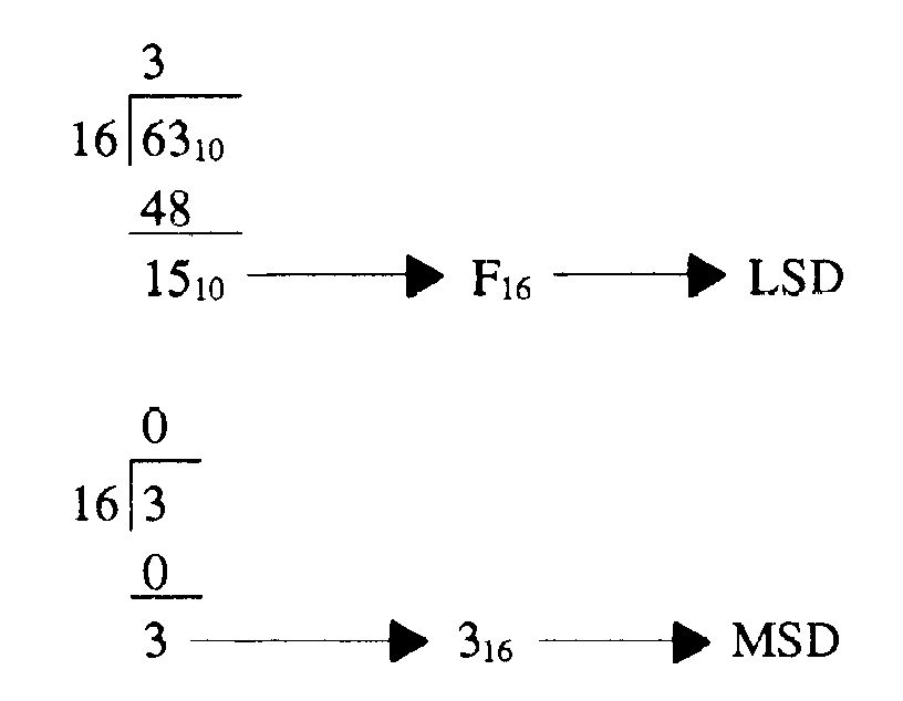
Decimal to Hex
To convert a decimal number to base 16, follow the repeated division procedures you used to convert to binary and octal, only divide by 16. Let’s look at an example:
Convert 6310 to hex:
Therefore, the hex equivalent of 6310 is 3F16.
You have to remember that the remainder is in base 10 and must be converted to hex if it exceeds 9. Let’s work through another example:
Convert 17410 to hex:
1-47
Write the solution from MSD to LSD:
AE16
There will probably be very few times when you will have to convert a decimal fraction to a hex fraction. If the occasion should arise, the conversion is done in the same manner as binary or octal. Use the following example as a pattern:
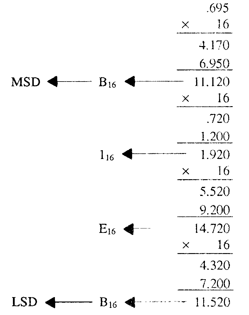
Convert 0.69510 to hex:
The solution: .B1EB16
Should you have the need to convert a decimal mixed number to hex, convert the whole number and the fraction separately; then recombine for the solution.
Convert the following decimal numbers to hex:
Q60. 4210. Q61. 8310. Q62. 17610 . Q63. 49110. Q64. 0.72110 (four places).
The converting of binary, octal, and hex numbers to their decimal equivalents is covered as a group later in this section.
1-48
BINARY CONVERSION
Earlier in this chapter, we mentioned that the octal and hex number systems are useful to computer programmers. It is much easier to provide data to a computer in one or the other of these systems. Likewise, it is important to be able to convert data from the computer into one or the other number systems for ease of understanding the data.
Binary to Octal
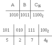
Look at the following numbers:
101110010011012
271158
You can easily see that the octal number is much easier to say. Although the two numbers look completely different, they are equal.
Since 8 is equal to 23, then one octal digit can represent three binary digits, as shown below:
With the use of this principle, the conversion of a binary number is quite simple. As an example, follow the conversion of the binary number at the beginning of this section.
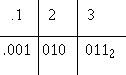
Write out the binary number to be converted. Starting at the radix point and moving left, break the binary number into groups of three as shown. This grouping of binary numbers into groups of three is called binary-coded octal (BCO). Add 0s to the left of any MSD that will fill a group of three:
Next, write down the octal equivalent of each group:
1-49
To convert a binary fraction to its octal equivalent, starting at the radix point and moving right, expand each digit into a group of three:
Add 0s to the right of the LSD if necessary to form a group of three. Now write the octal digit for each group of three, as shown below:
To convert a mixed binary number, starting at the radix point, form groups of three both right and left:
Convert the following binary numbers to octal:
Q65. 102. Q66. 10102. Q67. 1011112. Q68. 0.00112. Q69. 0.1100112. Q70. 110111.0101012.
Binary to Hex
The table below shows the relationship between binary and hex numbers. You can see that four binary digits may be represented by one hex digit. This is because 16 is equal to 24.
1-50
Using this relationship, you can easily convert binary numbers to hex. Starting at the radix point and moving either right or left, break the number into groups of four. The grouping of binary into four bit groups is called binary-coded hexadecimal (BCH).
Convert 1110100112 to hex:
Add 0s to the left of the MSD of the whole portion of the number and to the right of the LSD of the fractional part to form a group of four.
Convert .1112 to hex:
In this case, if a 0 had not been added, the conversion would have been .716, which is incorrect.
Convert the following binary numbers to hex:
Q71. 102. Q72. 10112. Q73. 1011112. Q74. 0.00112. Q75. 0.1100112.

1-51
Q76. 110111.0101012. OCTAL CONVERSION
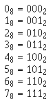
The conversion of one number system to another, as we explained earlier, is done to simplify computer programming or interpreting of data.
Octal to Binary
For some computers to accept octal data, the octal digits must be converted to binary. This process is the reverse of binary to octal conversion.
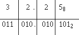
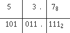
To convert a given octal number to binary, write out the octal number in the following format. We will convert octal 5678:
Next, below each octal digit write the corresponding three-digit binary-coded octal equivalent:
Solution: 5678 equals 101 110 1112
Remove the conversion from the format:
1011101112
As you gain experience, it may not be necessary to use the block format.
An octal fraction (.1238) is converted in the same manner, as shown below:
Solution: .1238 equals .0010100112
Apply these principles to convert mixed numbers as well.
Convert 32.258 to binary:
1-52
Solution: 32.258 equals 011010.0101012
Convert the following numbers to binary:
Q77. 738 Q78. 5128 Q79. 4038 Q80. 0.4568 Q81. 0.738 Q82. 36.58
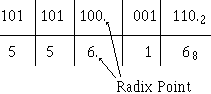
Octal to Hex
You will probably not run into many occasions that call for the conversion of octal numbers to hex. Should the need arise, conversion is a two-step procedure. Convert the octal number to binary; then convert the binary number to hex. The steps to convert 53.78 to hex are shown below:
Regroup the binary digits into groups of four and add zeros where needed to complete groups; then convert the binary to hex.
Solution: 53.78 equals 2B.E16
Convert the following numbers to hex:
Q83. 748 Q84. 5128 Q85. 0.038 Q86. 14.428
HEX CONVERSION
The procedures for converting hex numbers to binary and octal are the reverse of the binary and octal conversions to hex.
1-53
Hex to Binary
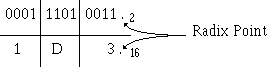
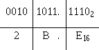
To convert a hex number to binary, set up the number in the block format you used in earlier conversions. Below each hex digit, write the four-digit binary equivalent. Observe the following example:
Convert ABC16 to binary:
Solution: ABC16 = 1010101111002
Hex to Octal
Just like the conversion of octal to hex, conversion of hex to octal is a two-step procedure. First, convert the hex number to binary; and second, convert the binary number to octal. Let’s use the same example we used above in the hex to binary conversion and convert it to octal:
Convert these base 16 numbers to their equivalent base 2 and base 8 numbers:
Q87. 2316 Q88. 1B16 Q89. 0.E416 Q90. 45.A16
CONVERSION TO DECIMAL
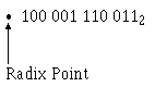
Computer data will have little meaning to you if you are not familiar with the various number systems. It is often necessary to convert those binary, octal, or hex numbers to decimal numbers. The need for understanding is better illustrated by showing you a paycheck printed in binary. A check in the amount of $10,010,101.002 looks impressive but in reality only amounts to $149.0010
1-54
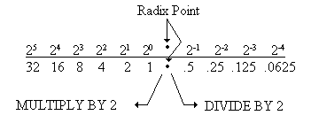
Binary to Decimal
The computer that calculates your pay probably operates with binary numbers, so a conversion takes place in the computer before the amount is printed on your check. Some computers, however, don’t automatically convert from binary to decimal. There may be times when you must convert mathematically.
To convert a base 2 number to base 10, you must know the decimal equivalent of each power of 2. The decimal value of a power of 2 is obtained by multiplying 2 by itself the number of times indicated by the exponent for whole numbers; for example, 24 = 2 · 2 · 2 · 2 or 1610.
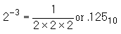
For fractional numbers, the decimal value is equal to 1 divided by 2 multiplied by itself the number of times indicated by the exponent. Look at this example:
The table below shows a portion of the positions and decimal values of the binary system:
Remember, earlier in this chapter you learned that any number to the 0 power is equal to 110.
Another method of determining the decimal value of a position is to multiply the preceding value by 2 for whole numbers and to divide the preceding value by 2 for fractional numbers, as shown below:
Let’s convert a binary number to decimal by using the positional notation method. First, write out the number to be converted; then, write in the decimal equivalent for each position with a 1 indicated. Add these values to determine the decimal equivalent of the binary number. Look at our example:
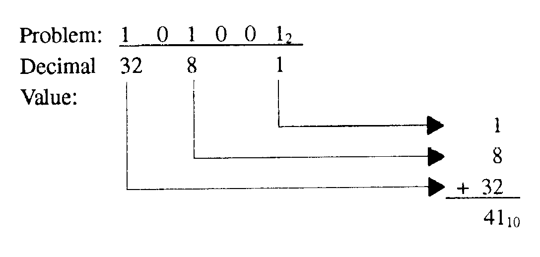
1-55
You may want to write the decimal equivalent for each position as we did in the following example. Add only the values indicated by a 1.
You should make sure that the decimal values for each position are properly aligned before adding. For practice let’s convert these binary numbers to decimal:
Q91. 100102 Q92. 11111002 Q93. 10101012 Q94. 0.01012 Q95. 0.10102 Q96. 1101101.11112
Octal to Decimal
Conversion of octal numbers to decimal is best done by the positional notation method. This process is the one we used to convert binary numbers to decimal.
First, determine the decimal equivalent for each position by multiplying 8 by itself the number of times indicated by the exponent. Set up a bar graph of the positions and values as shown below:
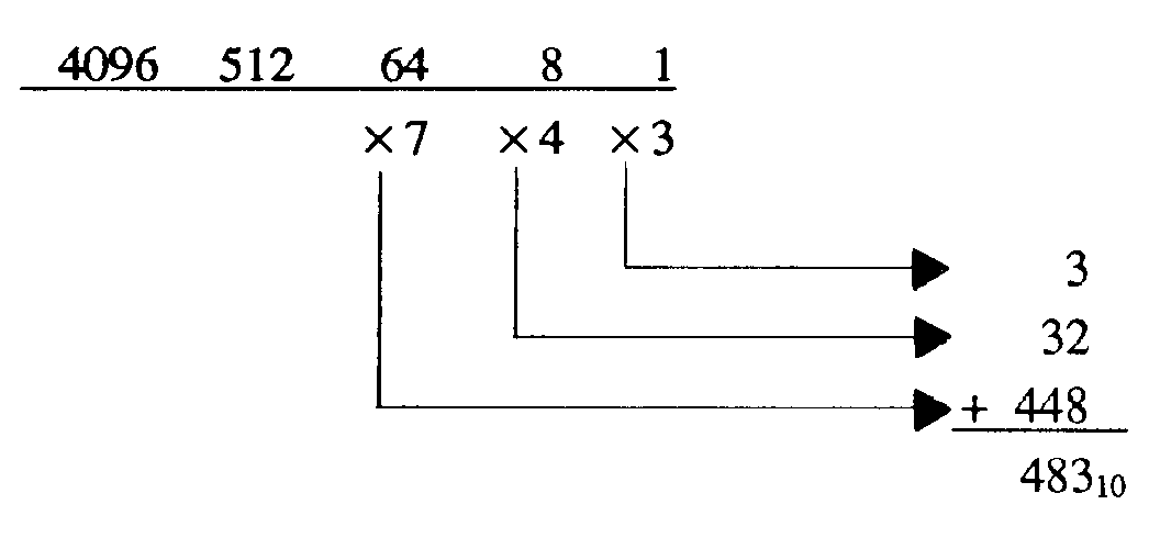
1-56
To convert an octal number to decimal, write out the number to be converted, placing each digit under the proper position.
Example:
Next, multiply the decimal equivalent by the corresponding digit of the octal number; then, add this column of figures for the final solution:
Solution: 7438 is equal to 48310
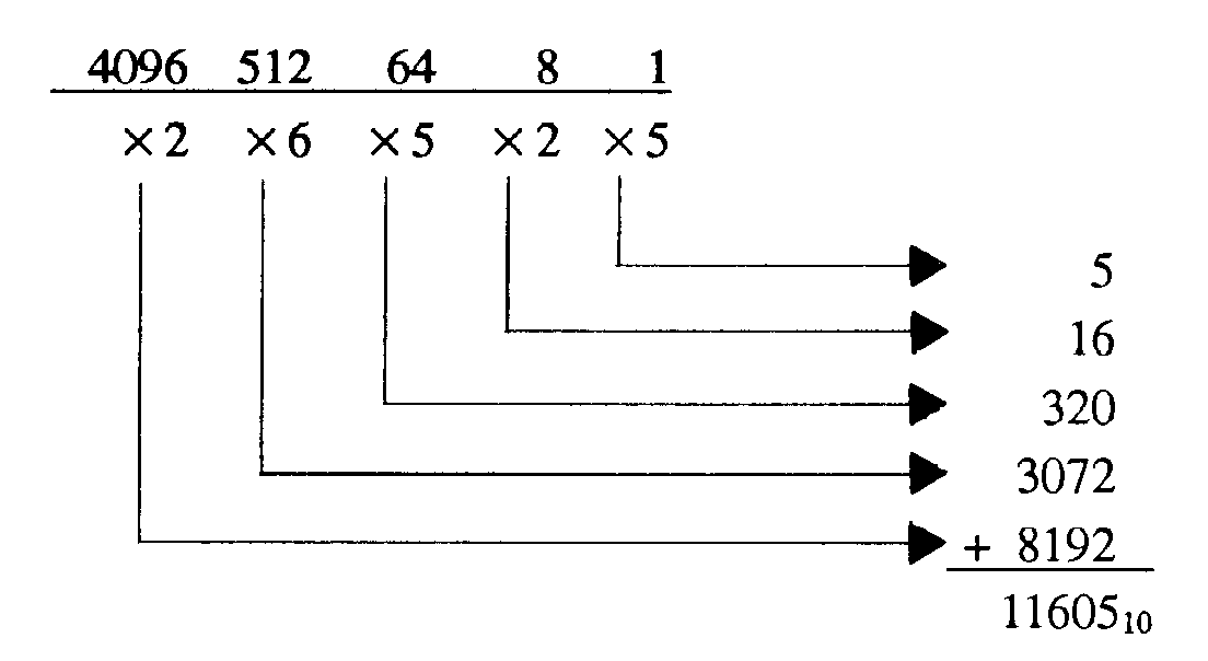
Now follow the conversion of 265258 to decimal:
Solution: 11,60510 is the decimal equivalent of 26,5258
To convert a fraction or a mixed number, simply use the same procedure.
Example: Change .58 to decimal:
1-57
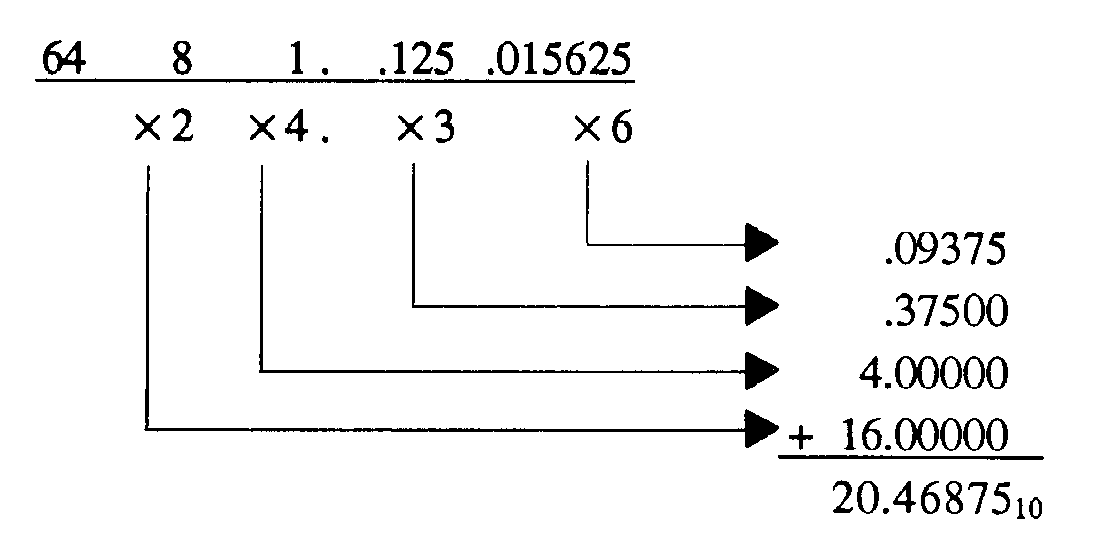
Example: Convert 24.368 to decimal:
Solution: 24.368 equals 20.4687510
If your prefer or find it easier, you may want to convert the octal number to binary and then to decimal.
Convert the following numbers to decimal:
Q97. 178 Q98. 648 Q99. 3758 Q100. 0.48 Q101. 0.61
8
Q102. 10.228
Hex to Decimal
It is difficult to comprehend the magnitude of a base 16 number until it is presented in base 10; for instance, E016 is equal to 22410. You must remember that usually fewer digits are necessary to represent a decimal value in base 16.
When you convert from base 16 to decimal, you may use the positional notation system for the powers of 16 (a bar graph). You can also convert the base 16 number to binary and then convert to base 10.
Note in the bar graph below that each power of 16 results in a tremendous increase in the decimal equivalent. Only one negative power (16 - 1) is shown for demonstration purposes:
1-58
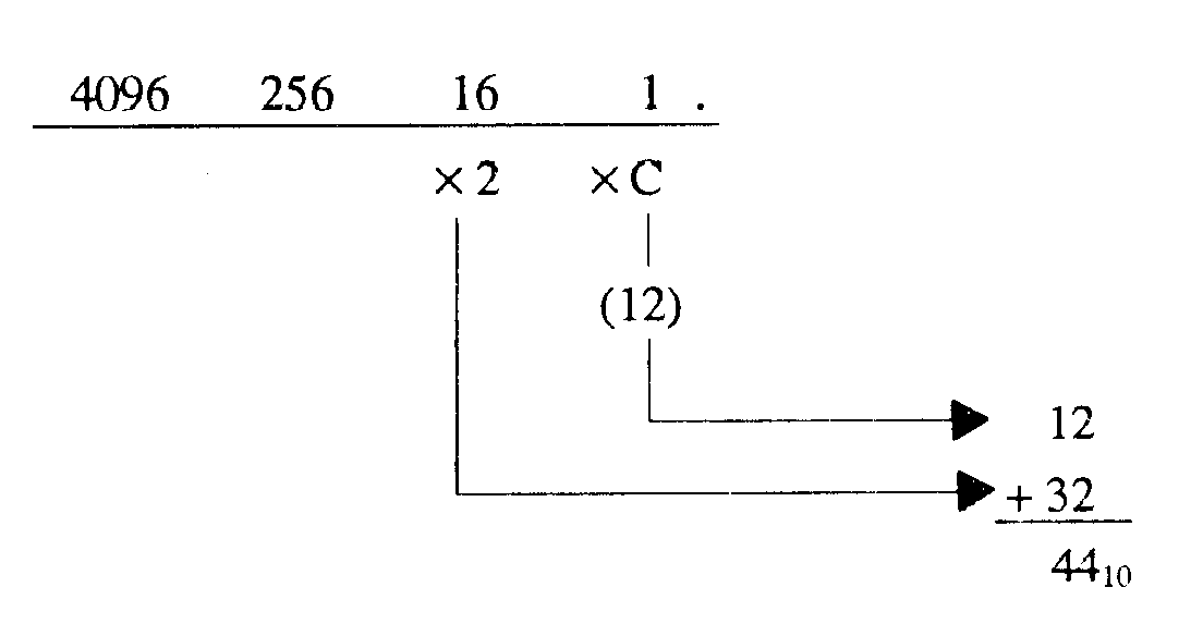
Just as you did with octal conversion, write out the hex number, placing each digit under the appropriate decimal value for that position. Multiply the decimal value by the base 16 digit and add the values. (Convert A through F to their decimal equivalent before multiplying). Let’s take a look at an example.
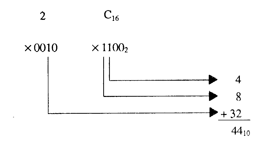
Convert 2C16 to decimal:
The decimal equivalent of 2C16 is 4410.
Use the same procedure we used with binary and octal to convert base 16 fractions to decimal.
If you choose to convert the hex number to binary and then to decimal, the solution will look like this:
Convert these base 16 numbers to base 10:
Q103. 2416 Q104. A516 Q105. DB16
1-59
Q106. 3E6.516
BINARY-CODED DECIMAL
In today’s technology, you hear a great deal about microprocessors. A microprocessor is an integrated circuit designed for two purposes: data processing and control.
Computers and microprocessors both operate on a series of electrical pulses called words. A word can be represented by a binary number such as 101100112. The word length is described by the number of digits or BITS in the series. A series of four digits would be called a 4-bit word and so forth. The most common are 4-, 8-, and 16-bit words. Quite often, these words must use binary-coded decimal inputs.
Binary-coded decimal, or BCD, is a method of using binary digits to represent the decimal digits 0 through 9. A decimal digit is represented by four binary digits, as shown below:
You should note in the table above that the BCD coding is the binary equivalent of the decimal digit.
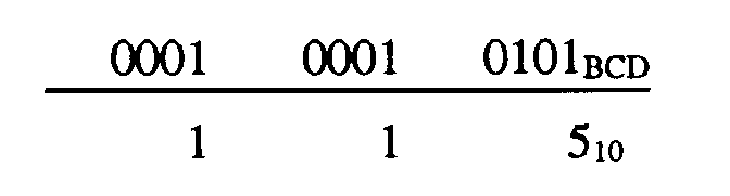
Since many devices use BCD, knowing how to handle this system is important. You must realize that BCD and binary are not the same. For example, 4910 in binary is 1100012, but 4910 in BCD is 01001001BCD. Each decimal digit is converted to its binary equivalent.
BCD Conversion
You can see by the above table, conversion of decimal to BCD or BCD to decimal is similar to the conversion of hexadecimal to binary and vice versa.
For example, let’s go through the conversion of 26410 to BCD. We’ll use the block format that you used in earlier conversions. First, write out the decimal number to be converted; then, below each digit write the BCD equivalent of that digit:
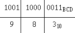
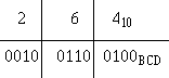
1-60
The BCD equivalent of 26410 is 001001100100BCD. To convert from BCD to decimal, simply reverse the process as shown:
BCD Addition
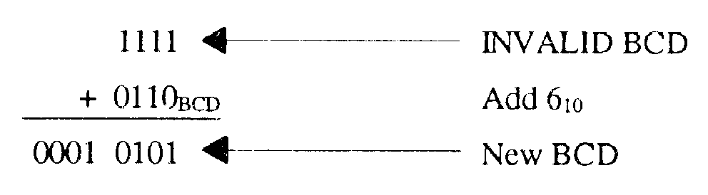
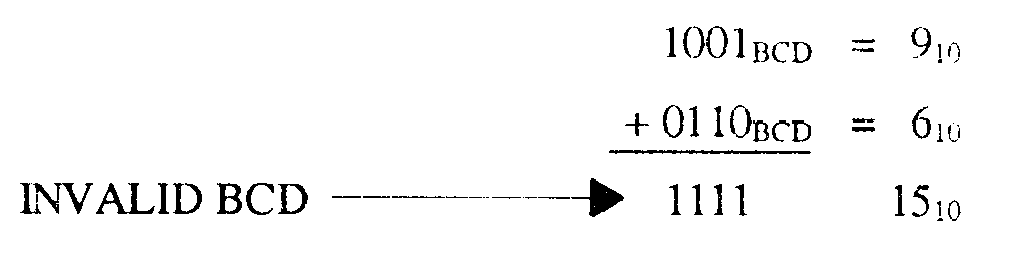
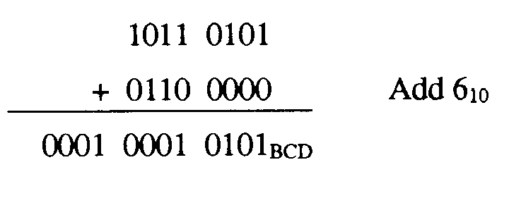
The procedures followed in adding BCD are the same as those used in binary. There is, however, the possibility that addition of BCD values will result in invalid totals. The following example shows this:
Add 9 and 6 in BCD:
The sum 11112 is the binary equivalent of 1510; however, 1111 is not a valid BCD number. You cannot exceed 1001 in BCD, so a correction factor must be made. To do this, you add 610 (0110BCD) to the sum of the two numbers. The "add 6" correction factor is added to any BCD group larger than 10012. Remember, there is no 10102, 10112, 11002, 11012, 11102, or 11112 in BCD:
The sum plus the add 6 correction factor can then be converted back to decimal to check the answer. Put any carries that were developed in the add 6 process into a new 4-bit word:
Now observe the addition of 6010 and 5510 in BCD:
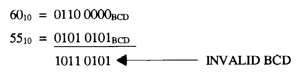
1-61
In this case, the higher order group is invalid, but the lower order group is valid. Therefore, the correction factor is added only to the higher order group as shown:
Convert this total to decimal to check your answer:
Remember that the correction factor is added only to groups that exceed 910 (1001BCD). Convert the following numbers to BCD and add:
Q107.
Q108.
Q109.
1-62
Q110.
SUMMARY
Now that you’ve completed this chapter, you should have a basic understanding of number systems. The number systems that were dealt with are used extensively in the microprocessor and computer fields. The following is a summary of the emphasized terms and points found in the "Number Systems" chapter.
The UNIT represents a single object. A NUMBER is a symbol used to represent one or more units.
The RADIX is the base of a positional number system. It is equal to the number of symbols used in that number system.
A POSITIONAL NOTATION is a system in which the value or magnitude of a number is defined not only by its digits or symbol value, but also by its position. Each position represents a power of the radix, or base, and is ranked in ascending or descending order.
The MOST SIGNIFICANT DIGIT (MSD) is a digit within a number (whole or fractional) that has the largest effect (weighing power) on that number.
The LEAST SIGNIFICANT DIGIT (LSD) is a digit within a number (whole or fractional) that has the least effect (weighting power) on that number.
1-63
The BINARY NUMBER SYSTEM is a base 2 system. The symbols 1 and 0 can be used to represent the state of electrical/electronic devices. A binary 1 may indicate the device is active; a 0 may indicate the device is inactive.
The OCTAL NUMBER SYSTEM is a base 8 system and is quite useful as a tool in the conversion of binary numbers. This system works because 8 is an integral power of 2; that is, 23 = 8. The use of octal numbers reduces the number of digits required to represent the binary equivalent of a decimal number.
The HEX NUMBER SYSTEM is a base 16 system and is sometimes used in computer systems. A binary number can be converted directly to a base 16 number if the binary number is first broken into groups of four digits.
The basic rules of ADDITION apply to each of the number systems. Each system becomes unique when carries are produced.
SUBTRACTION in each system is based on certain rules of that number system. The borrow varies in magnitude according to the number system in use. In most computers, subtraction is accomplished by using the complement (R’s or R’s-1) of the subtrahend and adding it to the minuend.
To CONVERT A WHOLE BASE 10 NUMBER to another system, divide the decimal number by the base of the number system to which you are converting. Continue dividing the quotient of the previous division until it can no longer be done. Extract the remainders ¾ the remainder from the first computation will yield the LSD; the last will provide the MSD.
1-64
To CONVERT DECIMAL FRACTIONS, multiply the fraction by the base of the desired number system. Extract those digits that move to the left of the radix point. Continue to multiply the fractional product for as many places as needed. The first digit left of the radix point will be the MSD, and the last will be the LSD. The example to the right shows the process of converting 248.3210 to the octal equivalent (370.2438).
BINARY numbers are converted to OCTAL and HEX by the grouping method. Three binary digits equal one octal digit; four binary digits equal one hex digit.
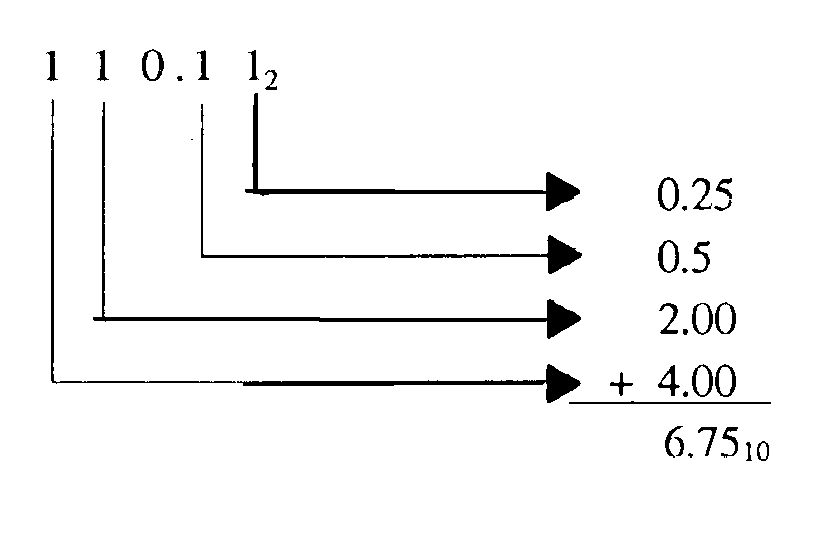
1-65
To CONVERT binary, octal, and hex numbers to DECIMAL use the POWERS of the base being converted.
BINARY-CODED DECIMAL (BCD) is a coding system used with some microprocessors. A correction factor is needed to correct invalid numbers
ANSWERS TO QUESTIONS Q1. THROUGH Q110. A1. Unit
A2. Number
A3. Arabic
A4. The number of symbols used in the system A5. 17310
A6. 103, 102, 101, 100,
A7. Radix point
A8.
(a) MSD - 4, LSD - 0
(b) MSD - 1, LSD - 6
(c) MSD - 2, LSD - 4 (d) MSD - 2, LSD - 1
A9. 111112
A10. 111012
A11. 1000012
A12. 101111 2
A13. 10002
1-66
A14. 110111102
A15. 100002
A16. 10112
A17. 111012
A18. 112
A19. 11102
A20. 111112
A21. 22110
A22. 011000112
A23. - 00012
A24. 108
A25. 608
A26. 10158
A27. 223068
A28. 1518
A29. 248
A30. 3218
A31. 368
A32. 3368
A33. 3778
A34. 1048
A35. 77678
A36. DD8D16
A37. 11FDB16
A38. 125F16
A39. 1202016
A40. 191AB16
A41. 1AA816
A42. 33516
1-67
A43. 93516
A44. 953116
A45. 36B316
A46. 10ABC16
A47. 42F0F16
A48. 10010002
A49. 11000012
A50. 111100112
A51. 0.11102
A52. 0.01012
A53. 10001.011012
A54. 78
A55. 538
A56. 7638
A57. 0.74678
A58. 0.002038
A59. 374.1278
A60. 2A16
A61. 5316
A62. B016
A63. 1EB16
A64. 0.B89316
A65. 28
A66. 128
A67. 578
A68. 0.148
A69. 0.638
A70. 67.258
A71. 216
1-68
A72. B16
A73. 2F16
A74. 0.316
A75. 0.CC16
A76. 37.5416
A77. 1110112
A78. 1010010102
A79. 1000000112
A80. 0.1001011102
A81. 0.1110112
A82. 11110.1012
A83. 3C16
A84. 14A16
A85. 0.0C16
A86. C.8816
A87. 1000112; 438
A88. 110112; 338
A89. 0.1110012; 0.718
A90. 1000101.1012; 105.58
A91. 1810
A92. 12410
A93. 8510
A94. 0.312510
A95. 0.62510
A96. 109.937510
A97. 1510
A98. 5210
A99. 25310
A100. 0.510
1-69
A101. 0.76562510
A102. 8.2812510
A103. 3610
A104. 16510
A105. 21910
A106. 998.312510
A107. 1000BCD
A108. 1001BCD
A109. 0001 0001BCD
A110. 0010 0010BCD
2-1
CHAPTER 2
FUNDAMENTAL LOGIC CIRCUITS
LEARNING OBJECTIVES
Upon completing this chapter, you should be able to do the following:
1. Identify general logic conditions, logic states, logic levels, and positive and negative logic as these terms and characteristics apply to the inputs and outputs of fundamental logic circuits.
2. Identify the following logic circuit gates and interpret and solve the associated Truth Tables:
a. AND
b. OR
c. Inverters (NOT circuits) d. NAND
e. NOR
3. Identify variations of the fundamental logic gates and interpret the associated Truth Tables.
4. Determine the output expressions of logic gates in combination.
5. Recognize the laws, theorems, and purposes of Boolean algebra.
INTRODUCTION
In chapter 1 you learned that the two digits of the binary number system can be represented by the state or condition of electrical or electronic devices. A binary 1 can be represented by a switch that is closed, a lamp that is lit, or a transistor that is conducting. Conversely, a binary 0 would be represented by the same devices in the opposite state: the switch open, the lamp off, or the transistor in cut-off.
In this chapter you will study the four basic logic gates that make up the foundation for digital equipment. You will see the types of logic that are used in equipment to accomplish the desired results. This chapter includes an introduction to Boolean algebra, the logic mathematics system used with digital equipment. Certain Boolean expressions are used in explanation of the basic logic gates, and their expressions will be used as each logic gate is introduced.
COMPUTER LOGIC
Logic is defined as the science of reasoning. In other words, it is the development of a reasonable or logical conclusion based on known information.
2-2
GENERAL LOGIC
Consider the following example: If it is true that all Navy ships are gray and the USS Lincoln is a Navy ship, then you would reach the logical conclusion that the USS Lincoln is gray.
To reach a logical conclusion, you must assume the qualifying statement is a condition of truth. For each statement there is also a corresponding false condition. The statement "USS Lincoln is a Navy ship" is true; therefore, the statement "USS Lincoln is not a Navy ship" is false. There are no in-between conditions.
Computers operate on the principle of logic and use the TRUE and FALSE logic conditions of a logical statement to make a programmed decision.
The conditions of a statement can be represented by symbols (variables); for instance, the statement "Today is payday" might be represented by the symbol P. If today actually is payday, then P is TRUE. If today is not payday, then P is FALSE. As you can see, a statement has two conditions. In computers, these two conditions are represented by electronic circuits operating in two LOGIC STATES. These logic states are 0 (zero) and 1 (one). Respectively, 0 and 1 represent the FALSE and TRUE conditions of a statement.
When the TRUE and FALSE conditions are converted to electrical signals, they are referred to as LOGIC LEVELS called HIGH and LOW. The 1 state might be represented by the presence of an electrical signal (HIGH), while the 0 state might be represented by the absence of an electrical signal (LOW).
If the statement "Today is payday" is FALSE, then the statement "Today is NOT payday" must be TRUE. This is called the COMPLEMENT of the original statement. In the case of computer math, complement is defined as the opposite or negative form of the original statement or variable. If today were payday, then the statement "Today is not payday" would be FALSE. The complement is shown by placing a bar, or VINCULUM, over the statement symbol (in this case, P ). This variable is spoken as NOT P. Table 2-1 shows this concept and the relationship with logic states and logic levels.
Table 2-1. ¾ Relationship of Digital Logic Concepts and Terms
Example 1: Assume today is payday
STATEMENT SYMBOL CONDITION LOGIC STATE
LOGIC LEVEL
Original: TODAY IS PAYDAY
P TRUE 1 HIGH
Complement: TODAY IS NOT PAYDAY P
FALSE 0 LOW
Example 2: Assume today is not payday
Original: TODAY IS NOT PAYDAY
P FALSE 0 LOW
Complement: TODAY IS NOT PAYDAY P
TRUE 1 HIGH
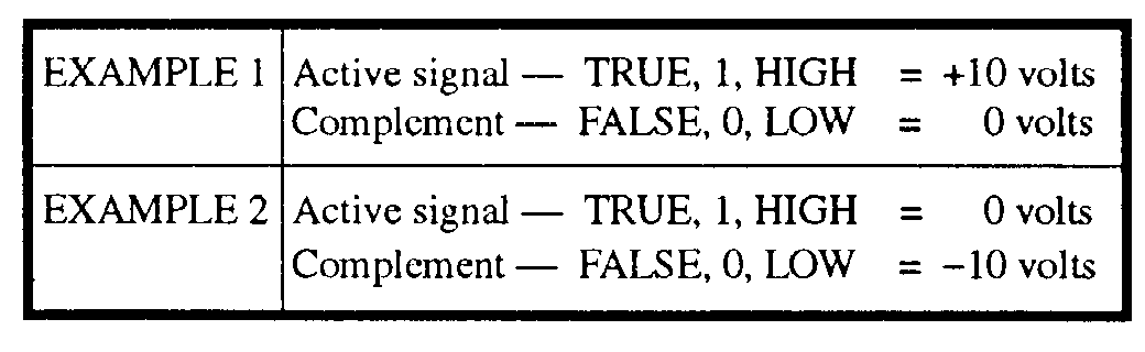
2-3
In some cases, more than one variable is used in a single expression. For example, the expression AB C D is spoken "A AND B AND NOT C AND D."
POSITIVE AND NEGATIVE LOGIC
To this point, we have been dealing with one type of LOGIC POLARITY, positive. Let’s further define logic polarity and expand to cover in more detail the differences between positive and negative logic.
Logic polarity is the type of voltage used to represent the logic 1 state of a statement. We have determined that the two logic states can be represented by electrical signals. Any two distinct voltages may be used. For instance, a positive voltage can represent the 1 state, and a negative voltage can represent the 0 state. The opposite is also true.
Logic circuits are generally divided into two broad classes according to their polarity ¾ positive logic and negative logic. The voltage levels used and a statement indicating the use of positive or negative logic will usually be specified on logic diagrams supplied by manufacturers.
In practice, many variations of logic polarity are used; for example, from a high-positive to a low- positive voltage, or from positive to ground; or from a high-negative to a low-negative voltage, or from negative to ground. A brief discussion of the two general classes of logic polarity is presented in the following paragraphs.
Positive Logic
Positive logic is defined as follows: If the signal that activates the circuit (the 1 state) has a voltage level that is more POSITIVE than the 0 state, then the logic polarity is considered to be POSITIVE. Table 2-2 shows the manner in which positive logic may be used.
Table 2-2. —Examples of Positive Logic
As you can see, in positive logic the 1 state is at a more positive voltage level than the 0 state.
Negative Logic
As you might suspect, negative logic is the opposite of positive logic and is defined as follows: If the signal that activates the circuit (the 1 state) has a voltage level that is more NEGATIVE than the 0 state, then the logic polarity is considered to be NEGATIVE. Table 2-3 shows the manner in which negative logic may be used.
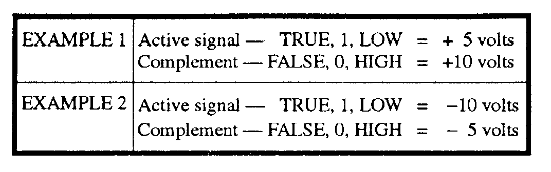
2-4
Table 2-3.—Examples of Negative Logic
NOTE: The logic level LOW now represents the 1 state. This is because the 1 state voltage is more negative than the 0 state.
In the examples shown for negative logic, you notice that the voltage for the logic 1 state is more negative with respect to the logic 0 state voltage. This holds true in example 1 where both voltages are positive. In this case, it may be easier for you to think of the TRUE condition as being less positive than the FALSE condition. Either way, the end result is negative logic.
The use of positive or negative logic for digital equipment is a choice to be made by design engineers. The difficulty for the technician in this area is limited to understanding the type of logic being used and keeping it in mind when troubleshooting.
NOTE:
UNLESS OTHERWISE NOTED, THE REMAINDER OF THIS BOOK WILL DEAL ONLY WITH POSITIVE LOGIC.
LOGIC INPUTS AND OUTPUTS
As you study logic circuits, you will see a variety of symbols (variables) used to represent the inputs and outputs. The purpose of these symbols is to let you know what inputs are required for the desired output.
If the symbol A is shown as an input to a logic device, then the logic level that represents A must be HIGH to activate the logic device. That is, it must satisfy the input requirements of the logic device before the logic device will issue the TRUE output.
Look at view A of figure 2-1. The symbol X represents the input. As long as the switch is open, the lamp is not lit. The open switch represents the logic 0 state of variable X.
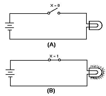
Figure 2-1. —Logic switch: A. Logic 0 state; B. Logic 1 state.
2-5
Closing the switch (view B), represents the logic 1 state of X. Closing the switch completes the circuit causing the lamp to light. The 1 state of X satisfied the input requirement and the circuit therefore produced the desired output (logic HIGH); current was applied to the lamp causing it to light.
If you consider the lamp as the output of a logic device, then the same conditions exist. The TRUE (1 state) output of the logic device is to have the lamp lit. If the lamp is not lit, then the output of the logic device is FALSE (0 state).
As you study logic circuits, it is important that you remember the state (1 or 0) of the inputs and outputs.
So far in this chapter, we have discussed the two conditions of logical statements, the logic states representing these two conditions, logic levels and associated electrical signals and positive and negative logic. We are now ready to proceed with individual logic device operations. These make up the majority of computer circuitry.
As each of the logic devices are presented, a chart called a TRUTH TABLE will be used to illustrate all possible input and corresponding output combinations. Truth Tables are particularly helpful in understanding a logic device and for showing the differences between devices.
The logic operations you will study in this chapter are the AND, OR, NOT, NAND, and NOR. The devices that accomplish these operations are called logic gates, or more informally, gates. These gates are the foundation for all digital equipment. They are the "decision-making" circuits of computers and other types of digital equipment. By making decisions, we mean that certain conditions must exist to produce the desired output.
In studying each gate, we will introduce various mathematical SYMBOLS known as BOOLEAN ALGEBRA expressions. These expressions are nothing more than descriptions of the input requirements necessary to activate the circuit and the resultant circuit output.
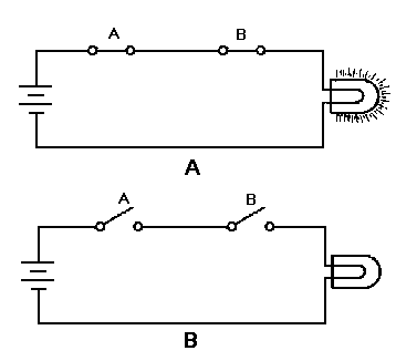
Figure 2-2. —AND gate.
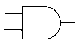
Figure 2-3.—AND gate equivalent circuit: A. Logic 1 state; B. Logic 0 state.
2-6
THE AND GATE
The AND gate is a logic circuit that requires all inputs to be TRUE at the same time in order for the output to be TRUE.
LOGIC SYMBOL
The standard symbol for the AND gate is shown in figure 2-2. Variations of this standard symbol may be encountered. These variations become necessary to illustrate that an AND gate may have more than one input.
If we apply two variables, A and B, to the inputs of the AND gate, then both A and B would have to be TRUE at the same time to produce the desired TRUE output. . The symbol f designates the output function. The Boolean expression for this operation is f = A·B or f = AB. The expression is spoken, "f = A AND B." The dot, or lack of, indicates the AND function.
AND GATE OPERATION
We can demonstrate the operation of the AND gate with a simple circuit that has two switches in series as shown in figure 2-3. You can see that both switches would have to be closed at the same time to light the lamp (view A). Any other combination of switch positions (view B) would result in an open circuit and the lamp would not light (logic 0).
Now look at figure 2-4. Signal A is applied to one input of the AND gate and signal B to the other. At time T0, both inputs are LOW (logic 0) and f is LOW. At T1, A goes HIGH (logic 1); B remains LOW; and as a result, f remains LOW. At T2, A goes LOW and B goes HIGH; f, however, is still LOW, because the proper input conditions have not been satisfied (A and B both HIGH at the same time). At T4, both A
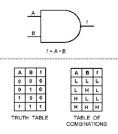
Figure 2-4. —AND gate input and output signals.
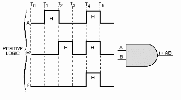
Figure 2-5. —AND gate logic symbol, Truth Table, and Table of Combinations.
2-7
and B are HIGH. As a result, f is HIGH. The input requirements have been satisfied, so the output is HIGH (logic 1).
TRUTH TABLE
Now let’s refer to figure 2-5. As you can see, a Truth Table and a Table of Combinations are shown. The latter is a deviation of the Truth Table. It uses the HIGH and LOW logic levels to depict the gate’s inputs and resultant output combinations rather than the 1 and 0 logic states. By comparing the inputs and outputs of the two tables, you see how one can easily be converted to the other (remember, 1 = HIGH and 0 = LOW). The Table of Combinations is shown here only to familiarize you with its existence, it will not be seen again in this book. As we mentioned earlier, the Truth Table is a chart that shows all possible combinations of inputs and the resulting outputs. Compare the AND gate Truth Table (figure 2-5) with the input signals shown in figure 2-4.
2-8
The first combination (A = 0, B = 0) corresponds to T0 in figure 2-4; the second to T1; the third to T2; and the last to T4. When constructing a Truth Table, you must include all possible combinations of the inputs, including the all 0s combination.
A Truth Table representing an AND gate with three inputs (X, Y, and Z) is shown below. Remember that the two-input AND gate has four possible combinations, with only one of those combinations providing a HIGH output. An AND gate with three inputs has eight possible combinations, again with only one combination providing a HIGH output. Make sure you include all possible combinations. To check if you have all combinations, raise 2 to the power equal to the number of input variables. This will give you the total number of possible combinations. For example:
EXAMPLE 1-AB = 22 = 4 combinations
EXAMPLE 2-XYZ = 23 = 8 combinations
X Y Z f 0 0 0 0 0 0 1 0 0 1 0 0 0 1 1 0 1 0 0 0 1 0 1 0 1 1 0 0 1 1 1 1
f = XYZ
As with all AND gates, all the inputs must be HIGH at the same time to produce a HIGH output. Don’t be confused if the complement of a variable is used as an input. When a complement is indicated as an input to an AND gate, it must also be HIGH to satisfy the input requirements of the gate. The Boolean expression for the output is formulated based on the TRUE inputs that give a TRUE output. Here is an adage that might help you better understand the AND gate:
In order to produce a 1 output, all the inputs must be 1. If any or all of the inputs is/are 0, then the output will be 0.
Referring to the following examples should help you cement this concept in your mind. Remember, the inputs, whether the original variable or the complement must be high in order for the output to be high. The three examples given are all AND gates with two inputs. Keep in mind the Boolean expression for the output is the result of all the inputs being HIGH.
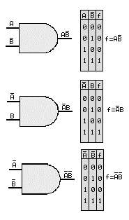
Figure 2-5a. —AND gate logic with two inputs, Truth Table.
2-9
You will soon be able to recognize the Truth Table for the other types of logic gates without having to look at the logic symbol.
Q1. What is defined as "the science of reasoning?" Q2. With regard to computer logic circuits, what is meant by "complement?" Q3. What are the complements of the following terms?
a. Q b. R
c. V
d. Z
Q4. If logic 1 = - 5 vdc and logic 0 = - 10 vdc, what logic polarity is being used? Q5. If logic 1 = +2 vdc and logic 0 = - 2 vdc, what logic polarity is being used? Q6. If logic 1 = - 5 vdc and logic 0 = 0 vdc, what logic polarity is being used? Q7. What is the Boolean expression for the output of an AND gate that has R and S as inputs? Q8. What must be the logic state of R and S to produce the TRUE output? Q9. How many input combinations exist for a four-input AND gate?
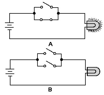
Figure 2-6. —OR gate.
2-10
THE OR GATE
The OR gate differs from the AND gate in that only ONE input has to be HIGH to produce a HIGH output. An easy way to remember the OR gate is that any HIGH input will yield a HIGH output.
LOGIC SYMBOL
Figure 2-6shows the standard symbol for the OR gate. The number of inputs will vary according to the needs of the designer.
The OR gate may also be represented by a simple circuit as shown in figure 2-7. In the OR gate, two switches are placed in parallel. If either or both of the switches are closed (view A), the lamp will light. The only time the lamp will not be lit is when both switches are open (view B).
Let’s assume we are applying two variables, X and Y, to the inputs of an OR gate. For the circuit to produce a HIGH output, either variable X, variable Y, or both must be HIGH. The Boolean expression for this operation is f = X+Y and is spoken "f equals X OR Y." The plus sign indicates the OR function and should not be confused with addition.
OR GATE OPERATION
Look at figure 2-8. At time T0, both X and Y are LOW and f is LOW. At T1, X goes HIGH producing a HIGH output. At T2 when both inputs go LOW, f goes LOW. When Y goes HIGH at T3, f
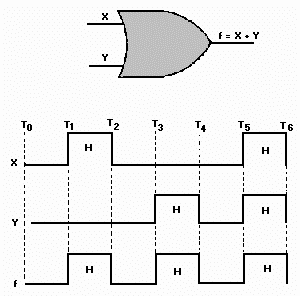
Figure 2-8. —OR gate input and output signals.
2-11
also goes HIGH and remains HIGH until both inputs are again LOW. At T5, both X and Y go HIGH causing f to go HIGH.
TRUTH TABLE
Using the inputs X and Y, let’s construct a Truth Table for the OR gate. You can see from the discussion of figure 2-8 that there are four combinations of inputs. List each of these combinations of inputs and the respective outputs and you have the Truth Table for the OR gate.
X Y f 0 0 0 0 1 1 1 0 1 1 1 1
f = X + Y
When writing or stating the Boolean expression for an OR gate with more than two inputs, simply place the OR sign (+) between each input and read or state the sign as OR. For example, the Boolean expression for an OR gate with the inputs of A, B, C, and D would be:
f = A+B+C+D
This expression is spoken "f equals A OR B OR C OR D."
You can substitute the complements for the original statements as we did with the AND gate or use negative logic; but for an output from an OR gate, at least one of the inputs must be TRUE.
2-12
Q10. Write the Boolean expression for an OR gate having G, K, and L as inputs. Q11. How many input combinations are possible using G, K, and L? Q12. How many of those combinations will produce a HIGH output?
THE INVERTER
The INVERTER, often referred to as a NOT gate, is a logic device that has an output opposite of the input. It is sometimes called a NEGATOR. It may be used alone or in combination with other logic devices to fulfill equipment requirements.
When an inverter is used alone, it is represented by the symbol shown in figure 2-9 (view A). It will more often be seen in conjunction with the symbol for an amplifier (view B). Symbols for inverters used in combination with other devices will be shown later in the chapter.
Let’s go back to the statement "Today is payday." We stated that P represents the TRUE state. If we apply P to the input of the inverter as shown in figure 2-10, then the output will be the opposite of the input. The output, in this case, is P . At times T0 through T2, P is LOW. Consequently, the output ( P ) is HIGH. At T2, P goes HIGH and as a result P goes LOW. P remains LOW as long as P is HIGH and vice versa. The Boolean expression for the output of this gate is f = P .
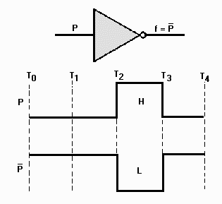
Figure 2-10. —Inverter input and resultant output.
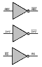
2-13
You will recall that P is the complement of P.
The Truth Table for an inverter is shown below.
P f 0 1 1 0
The output of an inverter will be the complement of the input. The following examples show various inputs to inverters and the resulting outputs:
The vinculum, or NOT sign, is placed over the entire output or removed from the output, depending on the input. If we applied A B C to an inverter, the output would be CBA . And if we ran that output through another inverter, the output would be A B C
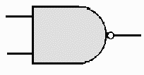
Figure 2-11. —NAND gate.
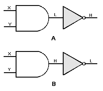
Figure 2-12. —NAND gate equivalent circuit: A. Either X or Y or both are LOW; B. Both X and Y are HIGH.
2-14
Q13. What is the complement of XYZ?
Q14. The input to an inverter is X + (YZ). What is the output
Q15. In a properly functioning circuit, can both the input and output of an inverter be HIGH at the same time?
THE NAND GATE
The NAND gate is another logic device commonly found in digital equipment. This gate is simply an AND gate with an inverter (NOT gate) at the output. LOGIC SYMBOL
The logic symbol for the NAND gate is shown in figure 2-11.
The NAND gate can have two or more inputs. The output will be LOW only when all the inputs are HIGH. Conversely, the output will be HIGH when any or all of the inputs are LOW.
The NAND gate performs two functions, AND and NOT. Separating the NAND symbol to show these two functions would reveal the equivalent circuits depicted in figure 2-12. This should help you better understand how the NAND gate functions.

Figure 2-13. —NAND gate input and output signals.
2-15
Inputs X and Y are applied to the AND gate. If either X or Y or both are LOW (view A), then the output of the AND gate is LOW. A LOW (logic 0) on the input of the inverter results in a HIGH (logic 1) output. When both X and Y are HIGH (view B), the output of the AND gate is HIGH; thus the output of the inverter is LOW. The Boolean expression for the output of a NAND gate with these inputs is f = XY . The expression is spoken "X AND Y quantity NOT." The output of any NAND gate is the negation of the input. For example, if our inputs are X and Y , the output will be YX .
NAND GATE OPERATION
Now, let’s observe the logic level inputs and corresponding outputs as shown in figure 2-13. At time T0, X and Y are both LOW. The output is HIGH; the opposite of an AND gate with the same inputs. At T1, X goes HIGH and Y remains LOW. As a result, the output remains HIGH. At T2, X goes LOW and Y goes HIGH. Again, the output remains HIGH. When both X and Y are HIGH at T4, the output goes LOW. The output will remain LOW only as long as both X and Y are HIGH.
TRUTH TABLE
The Truth Table for a NAND gate with X and Y as inputs is shown below.
X Y f 0 0 1 0 1 1 1 0 1 1 1 0
F = XY
Q16. A NAND gate has Z and X as inputs. What will be the output logic level if Z is HIGH and X is LOW?
Q17. What must be the state of the inputs to a NAND gate in order to produce a LOW output?
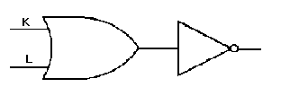
Figure 2-14. —NOR gate.
2-16
Q18. What is the output Boolean expression for a NAND gate with inputs A, B , and C?
Q19. A NAND gate has inputs labeled as A, B , and C. If A and B are HIGH, C must be at what logic level to produce a HIGH output?
THE NOR GATE
As you might expect, the NOR gate is an OR gate with an inverter on the output.
LOGIC SYMBOL
The standard logic symbol for this gate is shown in figure 2-14. More than just the two inputs may be shown.
The NOR gate will have a HIGH output only when all the inputs are LOW.
When broken down, the two functions performed by the NOR gate can be represented by the equivalent circuit depicted in figure 2-15. When both inputs to the OR gate are LOW, the output is LOW. A LOW applied to an inverter gives a HIGH output. If either or both of the inputs to the OR gate are HIGH, the output will be HIGH. When this HIGH output is applied to the inverter, the resulting output is LOW. The Boolean expression for the output of this NOR gate is f = K L+ . The expression is spoken, "K OR L quantity NOT."
NOR GATE OPERATION
The logic level inputs and corresponding outputs for a NOR gate are shown in figure 2-16. At time T0, both K and L are LOW; as a result, f is HIGH. At T1, K goes HIGH, L remains LOW, and f goes LOW. At T2, K goes LOW, L goes HIGH, and the output remains LOW. The output goes HIGH again at T3 when both inputs are LOW. At T4 when both inputs are HIGH, the output goes LOW and remains LOW until T5 when both inputs go LOW. Remember the output is just opposite of what it would be for an OR gate.
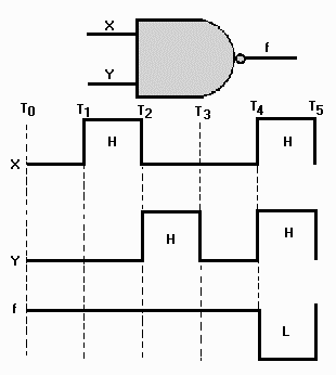
Figure 2-16. —NOR gate input and output signals.
2-17
TRUTH TABLE
The Truth Table for a NOR gate with K and L as inputs is shown below.
K L f 0 0 1 0 1 0 1 0 0 1 1 0
f = LK +
Q20. How does a NOR gate differ from an OR gate? Q21. What will be the output of a NOR gate when both inputs are HIGH? Q22. What is the output Boolean expression for a NOR gate with R and T as inputs? Q23. In what state must the inputs to a NOR gate be in order to produce a logic 1 output?
VARIATIONS OF FUNDAMENTAL GATES
Now that you are familiar with fundamental logic gates, let’s look at some variations of these gates that you may encounter.
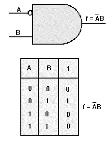
Figure 2-17. —AND gate with one inverted input.
2-18
Up to now you have seen inverters used alone or on the output of AND and OR gates. Inverters may also be used on one or more of the inputs to the logic gates. Take a look at the examples as discussed in the following paragraphs.
AND/NAND GATE VARIATIONS
If we place an inverter on one input of a two-input AND gate, the output will be quite different from that of the standard AND gate.
In figure 2-17, we have placed an inverter on the A input. When A is HIGH, the inverter makes it a LOW going into the AND gate. In order for the output to be HIGH, A would have to be LOW while B is HIGH, as shown in the Truth Table. If the inverter were on the B input, the output expression would then be f = A B .
Now let’s compare a NAND gate to an AND gate with an inverter on each input. Figure 2-18 shows these gates and the associated Truth Tables. With the NAND gate (view A), the output is HIGH when either or both inputs is/are LOW. The AND gate with inverters on each input (view B), produces a HIGH output only when both inputs are LOW. This comparison also points out the differences between the expressions f = A B (A AND B quantity NOT) and f = ¾fi¾ A B (NOT A AND NOT B).
Now, look over the Truth Tables for figures 2-17, 2-18, and 2-19; look at how the outputs vary with inverters in different positions.
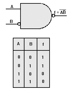
Figure 2-18. —Comparison of NAND gate and AND gate with inverted inputs: A. NAND gate; B. AND gate with inverters on each input.
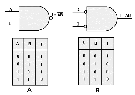
Figure 2-19. —NAND gate with one inverted input.
2-19
OR/NOR GATE VARIATIONS
The outputs of OR and NOR gates may also be changed with the use of inverters.
An OR gate with one input inverted is shown in figure 2-20. The output of this OR gate requires that A be LOW, B be HIGH, or both of these conditions existing at the same time in order to have a HIGH output. Since the A input is inverted, it must be LOW if B is LOW in order to produce a HIGH output. Therefore the output is f = A +B.
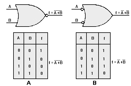
Figure 2-20. —OR gate with one inverted input.
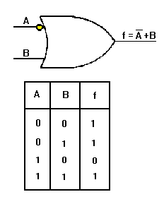
Figure 2-21. —Comparison of NOR gate and OR gate with inverted inputs: A. NOR gate; B. OR gate with inverters on both inputs.
2-20
Figure 2-21compares a NOR gate (view A), to an OR gate with inverters on both inputs (view B), and shows the respective Truth Tables. The NOR gate will produce a HIGH output only when both inputs are LOW. The OR gate with inverted inputs produces a HIGH output with all input combinations EXCEPT when both inputs are HIGH. This figure also illustrates the differences between the expressions f = A B+ (A OR B quantity NOT) and f = A + B (NOT A OR NOT B).
As with the NAND gate, one or more inputs to NOR gates may be inverted. Figure 2-22 shows the result of inverting a NOR gate input. In this case, because of the inversion of the B input and the inversion of the output, the only time this gate will produce a HIGH output is when A is LOW and B is HIGH. The output Boolean expression for this gate is f = BA + , spoken “A OR NOT B quantity NOT.”
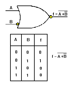
Figure 2-22. —NOR gate with one inverted input.
2-21
Table 2-4 illustrates AND, NOR, NAND, and OR gate combinations that produce the same output. You can see by the table that there is more than one way to achieve a desired output. Although the gates have only two inputs, the table can be extended to more than two inputs.
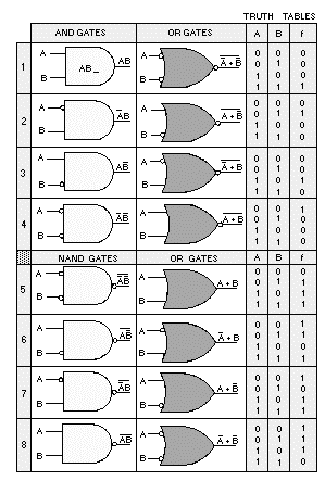
2-22
Table 2-4.—Equivalent AND and NOR, NAND and OR Gates
Q24. What is the output Boolean expression for an AND gate with A and B as inputs when the B input is inverted?
Q25. What is the equivalent logic gate of a two-input NAND gate with both inputs inverted?
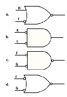
2-23
Q26. What is the output Boolean expression for the following gates?
LOGIC GATES IN COMBINATION
When you look at logic circuit diagrams for digital equipment, you are not going to see just a single gate, but many combinations of gates. At first it may seem confusing and complex. If you interpret one gate at a time, you can work your way through any network. In this section, we will analyze several combinations of gates and then provide you with some practice problems.
Figure 2-23 (view A) shows a simple combination of AND gates. The outputs of gates 1 and 2 are the inputs to gate 3. You already know that both inputs to an AND gate must be HIGH at the same time in order to produce a HIGH output.
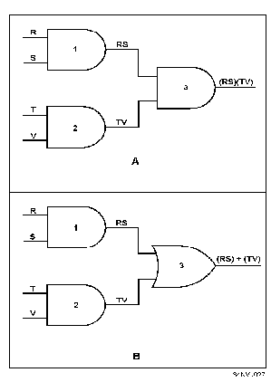
Figure 2-23. —Logic gate combinations: A. Simple combination of AND gates; B. Simple combination of AND gates and OR gate.
2-24
The output Boolean expression of gate 1 is RS, and the output expression of gate 2 is TV. These two output expressions become the inputs to gate 3. Remember, the output Boolean expression is the result of the inputs, in this case (RS)(TV); spoken "quantity R AND S AND quantity T AND V."
In view B we have changed gate 3 to an OR gate. The outputs of gates 1 and 2 remain the same but the output of gate 3 changes as you would expect. The output of gate 3 is now (RS)+(TV); spoken "quantity R AND S OR quantity T AND V."
In figure 2-24 (view A), the outputs of two OR gates are being applied as the input to third OR gate. The output for gate 1 is R+S, and the output for gate 2 is T+V. With these inputs, the output expression of gate 3 is (R+S)+(T+V).
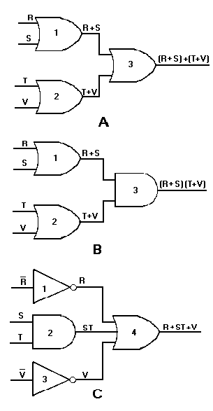
Figure 2-24. —Logic gate combinations: A. Simple combination of OR gates; B. Simple combination of OR gates and AND gate; C. Output expression without the parentheses.
2-25
In view B, gate 3 has been changed to an AND gate. The outputs of gates 1 and 2 do not change, but the output expression of gate 3 does. In this case, the gate 3 output expression is (R+S)(T+V). This expression is spoken, "quantity R OR S AND quantity T OR V." The parentheses are used to separate the input terms and to indicate the AND function. Without the parentheses the output expression would read R+ST+V, which is representative of the circuit in view C. As you can see, this is not the same circuit as the one depicted in view B. It is very important that the Boolean expressions be written and spoken correctly.
The Truth Table for the output expression of gate 3 (view B) will help you better understand the output. When studying this Truth Table, notice that the only time f is HIGH (logic 1) is when either or both R and S AND either or both T and V are HIGH (logic 1).
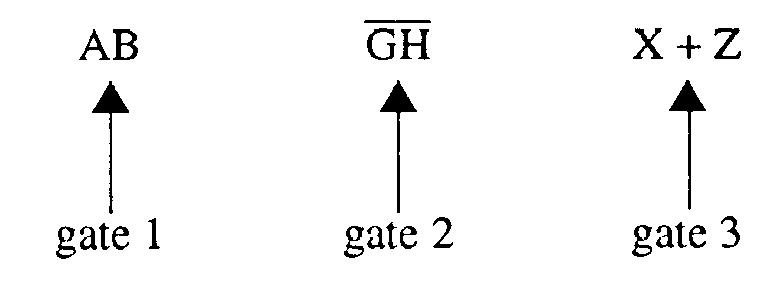
Figure 2-25. —Logic gate combinations.
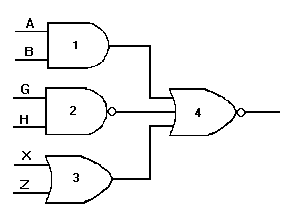
2-26
R S T V f 0 0 0 0 0 0 0 0 1 0 0 0 1 0 0 0 0 1 1 0 0 1 0 0 0 0 1 0 1 1 0 1 1 0 1 0 1 1 1 1 1 0 0 0 0 1 0 0 1 1 1 0 1 0 1 1 0 1 1 1 1 1 0 0 0 1 1 0 1 1 1 1 1 0 1 1 1 1 1 1
f = (R+S) (T+V)
Now let’s determine the output expression for the NOR gate in figure 2-25. First write the outputs of gates 1, 2, and 3:
Since all three outputs are applied to gate 4, proceed as you would for any NOR gate. We separate each input to gate 4 with an OR sign (+) and then place a vinculum over the entire expression. The output expression of gate 4 is:
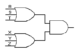
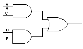
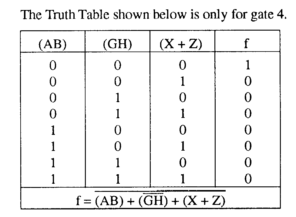
2-27
When you are trying to determine the outputs of logic gates in combination, take them one gate at a time!
Now write the output expressions for the following logic gate combinations: Q27.
Q28.
Q29.
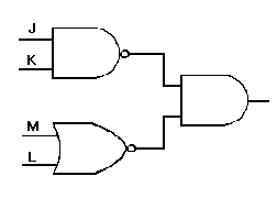
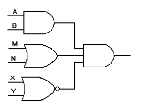
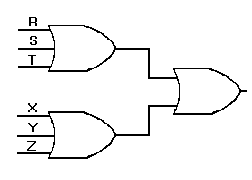
2-28
Q30.
Q31.
Q32.
BOOLEAN ALGEBRA
Boolean logic, or Boolean algebra as it is called today, was developed by an English mathematician, George Boole, in the 19th century. He based his concepts on the assumption that most quantities have two possible conditions ¾ TRUE and FALSE. This is the same theory you were introduced to at the beginning of this chapter.
Throughout our discussions of fundamental logic gates, we have mentioned Boolean expressions. A Boolean expression is nothing more than a description of the input conditions necessary to get the desired output. These expressions are based on Boole’s laws and theorems.
PURPOSE
Boolean algebra is used primarily by design engineers. Using this system, they are able to arrange logic gates to accomplish desired tasks. Boolean algebra also enables the engineers to achieve the desired output by using the fewest number of logic gates. Since space, weight, and cost are important factors in the design of equipment, you would usually want to use as few parts as possible.
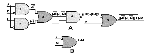
Figure 2-26. —Logic simplification: A. Complex series of gates; B. Simplified single OR gate.
2-29
Figure 2-26 (view A), shows a rather complex series of gates. Through proper application of Boolean algebra, the circuit can be simplified to the single OR gate shown in view B. Figure 2-27 shows the simplification process and the Boolean laws and theorem used to accomplish it.
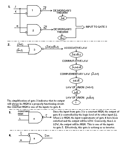
Figure 2-27. —Logic circuit simplification process.
2-30
LAWS AND THEOREMS
Each of the laws and theorems of Boolean algebra, along with a simple explanation, is listed below.
LAW OF IDENTITY ¾ a term that is TRUE in one part of an expression will be TRUE in all parts of the expression (A = A or A = A).
2-31
COMMUTATIVE LAW ¾ the order in which terms are written does not affect their value (AB = BA, A+B = B+A).
ASSOCIATIVE LAW ¾ a simple equality statement A(BC) = ABC or A+(B+C) = A+B+C. IDEMPOTENT LAW ¾ a term ANDed with itself or ORed with itself is equal to that term (AA =
A, A+A = A).
DOUBLE NEGATIVE LAW ¾ a term that is inverted twice is equal to the term A = A.
COMPLEMENTARY LAW ¾ a term ANDed with its complement equals 0, and a term ORed with its complement equals 1 (A A = 0, A+ A = 1).
LAW OF INTERSECTION ¾ a term ANDed with 1 equals that term and a term ANDed with 0 equals 0 (A·1 = A, A·0 = 0).
LAW OF UNION ¾ a term ORed with 1 equals 1 and a term ORed with 0 equals that term (A+1 = 1, A+0 = A).
DeMORGAN’S THEOREM ¾ this theorem consists of two parts: (1) AB = A + B and (2) BA + = A · B (Look at the fourth and eighth sets of gates in table 2-4). DISTRIBUTIVE LAW ¾ (1) a term (A) ANDed with an parenthetical expression (B+C) equals
that term ANDed with each term within the parenthesis: A·(B+C) = AB+AC; (2) a term (A) ORed with a parenthetical expression ( B ·C) equals that term ORed with each term within the parenthesis: A+(BC) = (A+B) · (A+C).
LAW OF ABSORPTION ¾ this law is the result of the application of several other laws: A·(A+B) = A or A+(AB) = A.
LAW OF COMMON IDENTITIES ¾ the two statements A·( A +B) = AB and A+ A B = A+B are based on the complementary law.
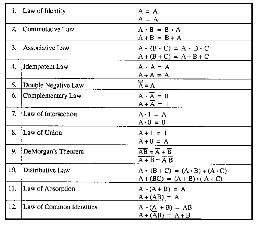
2-32
Table 2-5. —Boolean Laws and Theorems
If you wish a more detailed study of Boolean algebra, we suggest you obtain Mathematics, Volume 3, NAVEDTRA 10073-A1.
Q33. Boolean algebra is based on the assumption that most quantities have _______ conditions. Q34. Boolean algebra is used primarily by _______ to simplify circuits.
SUMMARY
This chapter has presented information on logic, fundamental logic gates, and Boolean laws and theorems. The information that follows summarizes the important points of this chapter.
LOGIC is the development of a logical conclusion based on known information.
Computers operate on the assumption that statements have two conditions ¾ TRUE and FALSE.
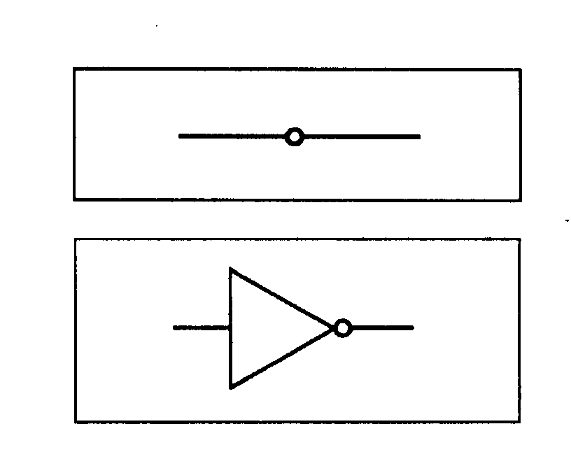

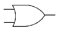
2-33
POSITIVE LOGIC is defined as follows: If the signal that activates the circuit (the 1 state) has a voltage level that is more POSITIVE than the 0 state, then the logic polarity is considered to be POSITIVE.
NEGATIVE LOGIC is defined as follows: If the signal that activates the circuit (the 1 state) has a voltage level that is more NEGATIVE than the 0 state, then the logic polarity is considered to be NEGATIVE.
In DIGITAL LOGIC (positive or negative), the TRUE condition of a statement is represented by the logic 1 state and the FALSE condition is represented by the logic 0 state.
LOGIC LEVELS High and LOW represent the voltage levels of the two logic states. Logic level HIGH represents the more positive voltage while logic level LOW represents the less positive (more negative) voltage. In positive logic, the HIGH level corresponds to the TRUE or 1 state and the LOW level corresponds to the FALSE or 0 state. In negative logic, the HIGH level corresponds to the FALSE or 0 state and the LOW level corresponds to the TRUE or 1 state.
A BOOLEAN EXPRESSION is a statement that represents the inputs and outputs of logic gates.
The AND GATE requires all inputs to be HIGH at the same time in order to produce a HIGH output.
The OR GATE requires one or both inputs to be HIGH in order to produce a HIGH output.
INVERTER (NOT function or negator) is a logic gate used to complement the state of the input variable; that is, a 1 becomes a 0 or a 0 becomes a 1. It may be used on any input or output of any gate to obtain the desired result.
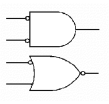
2-34
The NAND GATE functions as an AND gate with an inverted output.
The NOR GATE functions as an OR gate with an inverted output.
When deriving the output Boolean expression of a combination of gates, solve one gate at a time.
Boolean algebra is used primarily for the design and simplification of circuits.
ANSWERS TO QUESTIONS Q1. THROUGH Q34. A1. Logic.
A2. The opposite of the original statement. A3.
a. ,
b. ,
c. ,
d.
A4. Positive.
A5. Positive.
A6. Negative.
A7. f = RS. A8. Both must be 1s (HIGH) at the same time.
2-35
A9. 16.
A10. f = G+K+L. A11. Eight.
A12. Seven.
A13. XYZ
A14. X + (YZ). A15. No.
A16. HIGH.
A17. All inputs must be HIGH.
A18. CBA
A19. Low.
A20. It has an inverter on the output.
A21. Low.
A22. TR +
A23. All inputs must be low.
A24. A B .
A25. OR gate.
A26.
a. TR +
b. L K
c. G F
d. G F +
A27. (ABC)(DE). A28. (ABC)+(DE). A29. (R+S+T) (X+Y+Z). A30. (R+S+T)+(X+Y+Z).
A31. ( JK )( NM + ).
3-1
CHAPTER 3
SPECIAL LOGIC CIRCUITS
LEARNING OBJECTIVES
Upon completion of this chapter, you should be able to do the following:
1. Recognize the types of special logic circuits used in digital equipment.
2. Identify exclusive OR and exclusive NOR circuits and interpret their respective Truth Tables.
3. Identify adder and subtracter circuits.
4. Identify the types of flip-flops used in digital equipment and their uses.
5. Identify counters, registers, and clock circuits.
6. Describe the elements that make up logic families ¾ RTL, DTL, TTL, CMOS.
INTRODUCTION
Figure 3-1 is a portion of a typical logic diagram. It is similar to the diagrams you will encounter as your study of digital circuitry progresses.
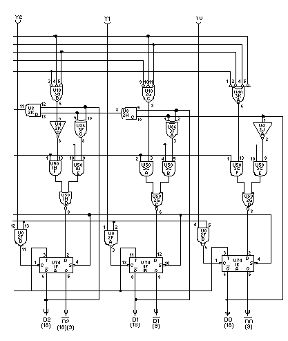
Figure 3-1. —Typical logic diagram.
3-2
Look closely at the figure. You will see many familiar logic gates. You will also see several that you may not recognize.
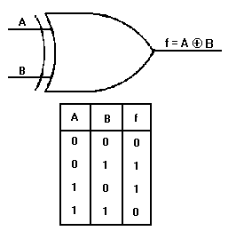
Figure 3-2. —Exclusive OR gate and Truth Table.
3-3
Digital equipment must be capable of many more operations than those described in chapter 2. Provisions must be made for accepting information; performing arithmetic or logic operations; and transferring, storing, and outputting information. Timing circuits are included to ensure that all operations occur at the proper time.
In this chapter you will become acquainted with the logic circuits used to perform the operations mentioned above.
THE EXCLUSIVE OR GATE
The exclusive OR gate is a modified OR gate that produces a HIGH output when only one of the inputs is HIGH. You will often see the abbreviation X-OR used to identify this gate. When both inputs are HIGH or when both inputs are LOW, the output is LOW.
The standard symbol for an exclusive OR gate is shown in figure 3-2 along with the associated Truth Table. The operation function sign for the exclusive OR gate is ¯ .
If you were to observe the input and output signals of an X-OR gate, the results would be similar to those shown in figure 3-3. At T0, both inputs are LOW and the output is LOW. At T1, A goes to HIGH and remains HIGH until T2. During this time the output is HIGH. At T3, B goes HIGH and remains HIGH through T5. At T4, A again goes HIGH and remains HIGH through T5. Between T3and T4 , the output is HIGH. At T4, when both A and B are HIGH, the output goes LOW.
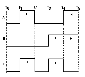
Figure 3-3. —Exclusive OR gate timing diagram.
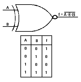
Figure 3-4. —Exclusive NOR gate and Truth Table.
3-4
THE EXCLUSIVE NOR GATE
The exclusive NOR (X-NOR) gate is nothing more than an X-OR gate with an inverted output. It produces a HIGH output when the inputs are either all HIGH or all LOW. The standard symbol and the Truth Table are shown in figure 3-4. The operation function sign is ¯ with a vinculum over the entire expression.
A timing diagram for the X-NOR gate is shown in figure 3-5. You can see that from T0 to T1, when both inputs are LOW, the output is HIGH. The output goes LOW when the inputs are opposite; one HIGH and the other LOW. At time T3, both inputs go HIGH causing the output to go HIGH.
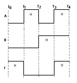
Figure 3-5. —Exclusive NOR gate timing diagram.
3-5
Q1. What is the sign of operation for the X-OR gate? Q2. What will be the output of an X-OR gate when both inputs are HIGH? Q3. A two-input X-OR gate will produce a HIGH output when the inputs are at what logic levels?
Q4. What type of gate is represented by the output Boolean expression RT ¯ ? Q5. What will be the output of an X-NOR gate when both inputs are LOW?
ADDERS
Adders are combinations of logic gates that combine binary values to obtain a sum. They are classified according to their ability to accept and combine the digits. In this section we will discuss quarter adders, half adders, and full adders.
QUARTER ADDER A quarter adder is a circuit that can add two binary digits but will not produce a carry. This circuit
will produce the following results:
0 plus 0 = 0
0 plus 1 = 1
1 plus 0 = 1
1 plus 1 = 0 (no carry)
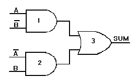
Figure 3-6. —Quarter adder.
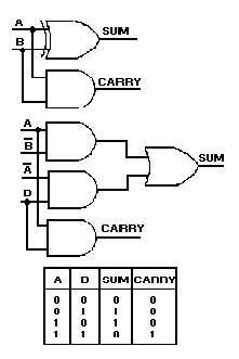
Figure 3-7. —Half adders and Truth Table.
3-6
You will notice that the output produced is the same as the output for the Truth Table of an X-OR. Therefore, an X-OR gate can be used as a quarter adder.
The combination of gates in figure 3-6 will also produce the desired results. When A and B are both LOW (0), the output of each AND gate is LOW (0); therefore, the output of the OR gate is LOW (0). When A is HIGH and B is LOW, then B is HIGH and AND gate 1 produces a HIGH output, resulting in a sum of 1 at gate 3. With A LOW and B HIGH, gate 2 output is HIGH, and the sum is 1. When both A and B are HIGH, neither AND gate has an output, and the output of gate 3 is LOW (0); no carry is produced.
HALF ADDER
A half adder is designed to combine two binary digits and produce a carry.
Figure 3-7 shows two ways of constructing a half adder. An AND gate is added in parallel to the quarter adder to generate the carry. The SUM column of the Truth Table represents the output of the quarter adder, and the CARRY column represents the output of the AND gate.
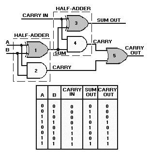
Figure 3-8. —Full adder and Truth Table.
3-7
We have seen that the output of the quarter adder is HIGH when either input, but not both, is HIGH. It is only when both inputs are HIGH that the AND gate is activated and a carry is produced. The largest sum that can be obtained from a half adder is 102 (12 plus 12). FULL ADDER
The full adder becomes necessary when a carry input must be added to the two binary digits to obtain the correct sum. A half adder has no input for carries from previous circuits.
One method of constructing a full adder is to use two half adders and an OR gate as shown in figure 3-8. The inputs A and B are applied to gates 1 and 2. These make up one half adder. The sum output of this half adder and the carry-from a previous circuit become the inputs to the second half adder. The carry from each half adder is applied to gate 5 to produce the carry-out for the circuit.
Now let’s add a series of numbers and see how the circuit operates.
First, let’s add 1 and 0. When either A or B is HIGH, gate 1 has an output. This output is applied to gates 3 and 4. Since the carry-in is 0, only gate 3 will produce an output. The sum of 12 and 0 is 12.
Now let’s add 12 and 12. If A and B are both HIGH, the output of gate 1 is LOW. When the carry-in is 0 (LOW), the output of gate 3 is LOW. Gate 2 produces an output that is applied to gate 5, which produces the carry-out. The sum of 12 and 12 is 102, just as it was for the half adder.
When A and B are both LOW and the carry-in is 1, only gate 3 has an output and produces a sum of 12 with no carry-out.
Now, let’s add A or B and a carry-in. For example, let’s assume that A is HIGH and B is LOW. With these conditions, gate 1 will have an output. This output and the carry-in applied to gates 3 and 4 will produce a sum out of 0 and a carry of 1. This carry from gate 4 will cause gate 5 to produce a carry-out. The sum of A and a carry (12 plus 12) is 102.
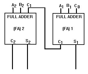
Figure 3-9. —Parallel binary adder.
3-8
When A, B, and the carry-in are all HIGH, a sum of 1 and a carry-out are produced. First, consider A and B. When both are HIGH, the output of gate 1 is LOW, and the output of gate 2 is HIGH, giving us a carry-out at gate 5. The carry-in produces a 1 output at gate 3, giving us a sum of 1. The output of the full adder is 112. The sum of 12 plus 12 plus 12 is 112.
PARALLEL ADDERS
The adders discussed in the previous section have been limited to adding single-digit binary numbers and carries. The largest sum that can be obtained using a full adder is 112.
Parallel adders let us add multiple-digit numbers. If we place full adders in parallel, we can add two- or four-digit numbers or any other size desired.
Figure 3-9 uses STANDARD SYMBOLS to show a parallel adder capable of adding two, two-digit binary numbers. In previous discussions we have depicted circuits with individual logic gates shown. Standard symbols (blocks) allow us to analyze circuits with inputs and outputs only. One standard symbol may actually contain many and various types of gates and circuits. The addend would be input on the A inputs (A2 = MSD, A1 = LSD), and the augend input on the B inputs (B2 = MSD, B1 = LSD). For this explanation we will assume there is no input to C0 (carry from a previous circuit).
Now let’s add some two-digit numbers. To add 102 (addend) and 012 (augend), assume there are numbers at the appropriate inputs. The addend inputs will be 1 on A2 and 0 on A1. The augend inputs will be 0 on B2 and 1 on B1. Working from right to left, as we do in normal addition, let’s calculate the outputs of each full adder.
With A1 at 0 and B1 at 1, the output of adder 1 will be a sum (S1) of 1 with no carry (C1). Since A2 is 1 and B2 is 0, we have a sum (S2) of 1 with no carry (C2) from adder 1. To determine the sum, read the outputs (C2, S 2, and S1) from left to right. In this case, C2 = 0, S2 = 1, and S1 = 1. The sum, then, of 102 and 012 is 0112 or 112.
To add 112 and 012, assume one number is applied to A1 and A2, and the other to B1 and B2, as shown in figure 3-10. Adder 1 produces a sum (S1) of 0 and a carry (C1) of 1. Adder 2 gives us a sum (S2)
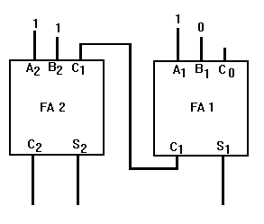
Figure 3-10. —Parallel addition.
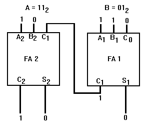
3-9
of 0 and a carry (C2) of 1. By reading the outputs (C2, S2, and S1), we see that the sum of 112 and 012 is 1002.
As you know, the highest binary number with two digits is 112. Using the parallel adder, let’s add 11
2 and 112.
First, apply the addend and augend to the A and B inputs. Calculate the output of each full adder beginning with full adder 1. With A1 and B1 at 1, S1 is 0 and C1 is 1. Since all three inputs (A2, B2, and C1) to full adder 2 are 1, the output will be 1 at S2 and 1 at C2. The output of the circuit, as you read left to right, is 1102, the sum of 112 and 112.
Parallel adders may be expanded by combining more full adders to accommodate the number of digits in the numbers to be added. There must be one full adder for each digit.
Q6. What advantage does a half adder have over a quarter adder? Q7. An X-OR gate may be used as what type of adder? Q8. What will be the output of a half adder when both inputs are 1s? Q9. What type of adder is used to handle a carry from a previous circuit? Q10. How many full adders are required to add four-digit numbers? Q11. With the inputs shown below, what will be the output of S1, S2, and C2?
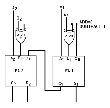
Figure 3-11. —R's complement adder/subtracter.
3-10
Q12. What is the output of C1? SUBTRACTION
Subtraction is accomplished in computers by the R’s complement and add method. This is the same method you used in chapter 1 to subtract binary numbers.
R’s complement subtraction allows us to use fewer circuits than would be required for separate add and subtract functions. Adding X-OR gates to full adders, as shown in figure 3-11, enables the circuit to perform R’s complement subtraction as well as addition.
To add two numbers using this circuit, the addend and augend are applied to the A and B inputs. The B inputs are applied to one input of the X-OR gates. A control signal is applied to the other input of the X-OR gates. When the control signal is LOW, the circuit will add; and when it is HIGH, the circuit will subtract.
In the add mode, the outputs of the X-OR gates will be the same as the B inputs. Addition takes place in the same manner as described in parallel addition.
Before we attempt to show subtraction, let’s review R’s complement subtraction. To subtract 102 from 112, write down the minuend (112). Perform the R’s complement on the subtrahend. Now add the minuend and the complemented subtrahend.
112 minuend
+ 102 R’s complement
101 Difference
Disregard the most significant 1, and the difference between 112 and 102 is 012. The most significant 1 will not be used in the example shown in the following paragraph.
3-11
Now let’s subtract 102 from 112 using the adder/subtracter circuit. The minuend (112) is input on the A terminals, and the subtrahend (102) is input on the B terminals. In the subtract mode, a 1 from the control circuit is input to each of the X-OR gates and to the C0 carry input. By applying a 1 to each of the X-OR gates, you find the output will be the complement of the subtrahend input at B1 and B2. Since B1 is a 0, the output of X-OR 1 will be 1. The input B2 to X-OR 2 will be inverted to a 0. The HIGH input to C0 acts as a carry from a previous circuit. The combination of the X-OR gates and the HIGH at C0 produces the R’s complement of the subtrahend. The full adders add the minuend and the R’s complement of the subtrahend and produce the difference. The output of C2 is not used. The outputs of S2 and S1 are 0 and 1, respectively, indicating a difference of 012. Therefore, 112 minus 102 equals 012.
Q13. What type of logic gates are added to a parallel adder to enable it to subtract? Q14. How many of these gates would be needed to add a four-digit number? Q15. In the add mode, what does the output of C2 indicate? Q16. In the subtract mode, a 1 at C0 performs what portion of the R’s complement? Q17. In the subtract mode, which portion of the problem is complemented?
FLIP-FLOPS
Flip-flops (FFs) are devices used in the digital field for a variety of purposes. When properly connected, flip-flops may be used to store data temporarily, to multiply or divide, to count operations, or to receive and transfer information.
Flip-flops are bistable multivibrators. The types used in digital equipment are identified by the inputs. They may have from two up to five inputs depending on the type. They are all common in one respect. They have two, and only two, distinct output states. The outputs are normally labeled Q and Q and should always be complementary. When Q = 1, then Q = 0 and vice versa.
In this section we will discuss four types of FFs that are common to digital equipment. They are the R-S, D, T, and J-K FFs.
R-S FLIP-FLOP
The R-S FF is used to temporarily hold or store information until it is needed. A single R-S FF will store one binary digit, either a 1 or a 0. Storing a four-digit binary number would require four R-S FFs.
The standard symbol for the R-S FF is shown in figure 3-12, view A. The name is derived from the inputs, R for reset and S for set. It is often referred to as an R-S LATCH. The outputs Q and Q are complements, as mentioned earlier.
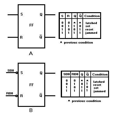
Figure 3-12. —R-S flip-flop: A. Standard symbol; B. R-S FF with inverted inputs.
3-12
The R-S FF has two output conditions. When the Q output is HIGH and Q is LOW, the FF is set. When Q is LOW and Q is HIGH, the FF is reset. When the R and S inputs are both LOW, the Q and Q outputs will both be HIGH. When this condition exists, the FF is considered to be JAMMED and the outputs cannot be used. The jammed condition is corrected when either S or R goes HIGH.
To set the flip-flop requires a HIGH on the S input and a LOW on the R input. To reset, the opposite is required; S input LOW and R input HIGH. When both R and S are HIGH, the FF will hold or "latch" the condition that existed before both inputs went HIGH.
Because the S input of this FF requires a logic LOW to set, a more easily understood symbol is shown in figure 3-12, view B. Refer to this view while reading the following paragraph.
In our description of R-S FF operation, let’s assume that the signals applied to the S and R inputs are the LSDs of two different binary numbers. Let’s also assume that these two binary numbers represent the speed and range of a target ship. The LSDs will be called SB0 (Speed Bit 0) and RB0 (Range Bit 0) and will be applied to the S and R inputs respectively. Refer to figure 3-12, view B, and figure 3-13. At time T0, both SB0 and RB0 are HIGH, as a result, both Q and Q are HIGH. This is the jammed state and as mentioned earlier, cannot be used in logic circuitry. At T1, SB0 goes LOW and RB0 remains HIGH; Q goes LOW and Q remains HIGH; the FF is reset. At T2 RB0 goes LOW and SB0 remains LOW; the FF is latched in the reset condition. At T3, SB0 goes HIGH and RB0 remains LOW; the FF sets. At T4 SB0 goes LOW and RB0 goes HIGH; the FF resets. When SB0 and RB0 input conditions reverse at T5, the FF sets. The circuit is put in the latch condition at T6 when SB0 goes LOW. Notice that the output changes states ONLY when the inputs are in opposite states.
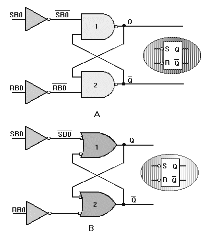
Figure 3-13. —R-S flip-flop with inverted inputs timing diagram.
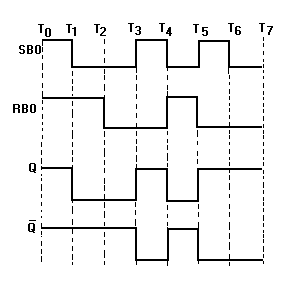
Figure 3-14. —R-S FF construction: A. Using cross-coupled NAND gates; B. Using cross-coupled OR gates.
3-13
Figure 3-14 shows two methods of constructing an R-S FF. We can use these diagrams to prove the Truth Table for the R-S FF.
3-14
Look at figure 3-14, view A. Let’s assume SB0 is HIGH and RB0 is LOW. You should remember from chapter 2 that the output of an inverter is the complement of the input. In this case, since SB0 is HIGH, SBO will be LOW. The LOW input to NAND gate 1 causes the Q output to go HIGH. This HIGH Q output is also fed to the input of NAND gate 2. The other input to NAND gate 2, RBO, is HIGH. With both inputs to gate 2 HIGH, the output goes LOW. The LOW Q output is also fed to NAND gate 1 to be used as the "latch" signal. If SB0 goes LOW while this condition exists, there will be no change to the outputs because the FF would be in the latched condition; both SB0 and RB0 LOW.
When RB0 is HIGH and SB0 is LOW, RBO being LOW drives the output, Q , to a HIGH condition. The HIGH Q and HIGH SBO inputs to gate 1 cause the output, Q, to go LOW. This LOW is also fed to NAND gate 2 to be used as the latch signal. Since SB0 is LOW, the FF will again go into the latched mode if RB0 goes LOW.
The cross-coupled OR gates in figure 3-14, view B, perform the same functions as the NAND gate configuration of view A. A HIGH input at SB0 produces a HIGH Q output, and a LOW at RB0 produces a LOW Q output. The cross-coupled signals ( Q to gate 1 and Q to gate 2) are used as the latch signals just as in view A. You can trace other changes of the inputs using your knowledge of basic logic gates.
Q18. What are R-S FFs used for? Q19. How many R-S FFs are required to store the number 1001012? Q20. For an R-S FF to change output conditions, the inputs must be in what states? Q21. How may R-S FFs be constructed?
TOGGLE FLIP-FLOP
The toggle, or T, flip-flop is a bistable device that changes state on command from a common input terminal.
The standard symbol for a T FF is illustrated in figure 3-15, view A. The T input may be preceded by an inverter. An inverter indicates a FF will toggle on a HIGH-to-LOW transition of the input pulse. The absence of an inverter indicates the FF will toggle on a LOW-to-HIGH transition of the pulse.
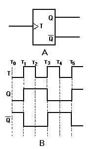
Figure 3-15. —Toggle (T) flip-flop: A. Standard symbol; B. Timing diagram.
3-15
The timing diagram in figure 3-15, view B, shows the toggle input and the resulting outputs. We will assume an initial condition (T0) of Q being LOW and Q being HIGH. At T1, the toggle changes from a LOW to a HIGH and the device changes state; Q goes HIGH and Q goes LOW. The outputs remain the same at T2 since the device is switched only by a LOW-to-HIGH transition. At T3, when the toggle goes HIGH, Q goes LOW and Q goes HIGH; they remain that way until T5.
Between T1 and T5, two complete cycles of T occur. During the same time period, only one cycle is observed for Q or Q . Since the output cycle is one-half the input cycle, this device can be used to divide the input by 2.
The most commonly used T FFs are J-K FFs wired to perform a toggle function. This use will be demonstrated later in this section.
Q22. How many inputs does a T FF have? Q23. What is the purpose of using T FFs?
D FLIP-FLOP
The D FF is a two-input FF. The inputs are the data (D) input and a clock (CLK) input. The clock is a timing pulse generated by the equipment to control operations. The D FF is used to store data at a predetermined time and hold it until it is needed. This circuit is sometimes called a delay FF. In other words, the data input is delayed up to one clock pulse before it is seen in the output.
The simplest form of a D FF is shown in figure 3-16, view A. Now, follow the explanation of the circuit using the Truth Table and the timing diagram shown in figure 3-16, views B and C.
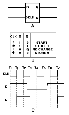
Figure 3-16. —D flip-flop: A. Standard symbol; B. Truth Table; C. Timing diagram.
3-16
Depending on the circuit design, the clock (CLK) can be a square wave, a constant frequency, or asymmetrical pulses. In this example the clock (CLK) input will be a constant input at a given frequency. This frequency is determined by the control unit of the equipment. The data (D) input will be present when there is a need to store information. Notice in the Truth Table that output Q reflects the D input only when the clock transitions from 0 to 1 (LOW to HIGH).
Let’s assume that at T0, CLK is 0, D is 1, and Q is 0. Input D remains at 1 for approximately 2 1/2 clock pulses. At T1, when the clock goes to 1, Q also goes to 1 and remains at 1 even though D goes to 0 between T2 and T3. At T3, the positive-going pulse of the clock causes Q to go to 0, reflecting the condition of D. The positive-going clock pulse at T5 causes no change in the output because D is still LOW. Between T5 and T6, D goes HIGH, but Q remains LOW until T7 when the clock goes HIGH.
The key to understanding the output of the D FF is to remember that the data (D) input is seen in the output only after the clock has gone HIGH.
You may see D FF symbols with two additional inputs ¾ CLR (clear) and PR (preset). These inputs are used to set the start condition of the FF ¾ CLR sets Q to 0; PR sets Q to 1. Figure 3-17 shows the standard symbol with the CLR and PR inputs. Since these inputs are preceded by inverters (part of the FF), a LOW-going signal is necessary to activate the FF. These signals (CLR and PR) override any existing condition of the output.
3-17
You may also see an inverter at the clock input. In this case, the output will change on the negative- going transition of the clock pulse.
Q24. What are the inputs to a D FF? Q25. How long is data delayed by a D FF? Q26. What condition must occur to have a change in the output of a D FF?
J-K FLIP-FLOP
The J-K FF is the most widely used FF because of its versatility. When properly used it may perform the function of an R-S, T, or D FF. The standard symbol for the J-K FF is shown in view A of figure 3-18.
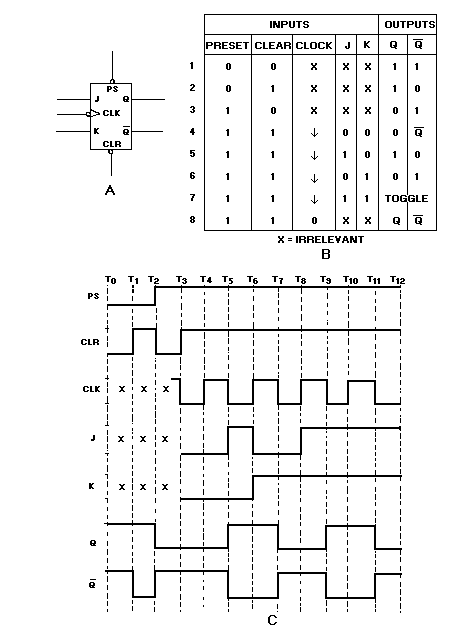
Figure 3-18. —J-K flip-flop: A. Standard symbol; B. Truth Table; C. Timing diagram.
3-18
The J-K is a five-input device. The J and K inputs are for data. The CLK input is for the clock; and the PS and CLR inputs are the preset and clear inputs, respectively. The outputs Q and Q are the normal complementary outputs.
Observe the Truth Table and timing diagram in figure 3-18, views B and C, as the circuit is explained.
3-19
Line 1 of the Truth Table corresponds to T0 in the timing diagram. The PS and CLR inputs are both LOW. The CLK, J, and K inputs are irrelevant. At this point the FF is jammed, and both Q and Q are HIGH. As with the R-S FF, this state cannot be used.
At T1, PS remains LOW while CLR goes HIGH. The Q output remains HIGH and Q goes LOW. The FF is in the PRESET condition (line 2 of the Truth Table).
At T2, PS goes HIGH, CLR goes LOW, Q goes LOW, and Q goes HIGH. At this point the FF is CLEARED (line 3 of the Truth Table). The condition of the CLK, J, and K inputs have no effect on the PS and CLR actions since these inputs override the other inputs. Starting at T3, PS and CLR will be held at HIGHs so as not to override the other actions of the FF. Using the PS and CLR inputs only, the circuit will function as an R-S FF.
Between T2 and T3, the CLK input is applied to the device. Since the CLK input has an inverter, all actions will take place on the negative-going transition of the clock pulse.
Line 4 of the Truth Table shows both PS and CLR HIGH, a negative-going CLK, and J and K at 0, or LOW. This corresponds to T3 on the timing diagram. In this condition the FF holds the previous condition of the output. In this case the FF is reset. If the circuit were set when these inputs occurred, it would remain set.
At time T5, we have a negative-going clock pulse and a HIGH on the J input. This causes the circuit to set, Q to go HIGH, and Q to go LOW. See line 5 of the Truth Table.
At T6, J goes LOW, K goes HIGH, and the clock is in a positive-going transition. There is no change in the output because all actions take place on the negative clock transition.
At T7, when J is LOW, K is HIGH; the clock is going negative, the FF resets, Q goes LOW, and Q goes HIGH (line 6).
With both J and K HIGH and a negative-going clock (as at T9 and line 7), the FF will toggle or change state with each clock pulse. It will continue to toggle as long as J and K both remain HIGH.
Line 8 of the Truth Table indicates that as long as the clock is in any condition other than a negative- going transition, there will be no change in the output regardless of the state of J or K.
As mentioned at the beginning of this section, J-K FFs may be used as R-S, T, or D FFs.
Figure 3-19 shows how a J-K can be made to perform the other functions.
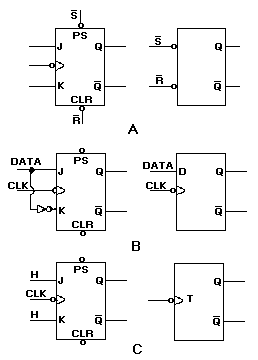
Figure 3-19. —J-K versatility: A. Using just the PS and CLR inputs; B. Data applied to the J input; C. Both J and K inputs held HIGH.
3-20
In view A, using just the PS and CLR inputs of the J-K will cause it to react like an R-S FF. In view B, data is applied to the J input. This same data is applied to the K input through an inverter
to ensure that the K input is in the opposite state. In this configuration, the J-K performs the same function as a D FF.
View C shows both the J and K inputs held at 1, or HIGH. The FF will change state or toggle with each negative-going transition of the clock just as a T FF will.
Now you can see the versatility of the J-K FF.
Q27. What type of FF can be used as an R-S, a T, or a D FF? Q28. What will be the output of Q if J is HIGH, PS and CLR are HIGH, and the clock is going
negative?
Q29. Assume that K goes HIGH and J goes LOW; when will the FF reset? Q30. What logic levels must exist for the FF to be toggled by the clock? Q31. What two inputs to a J-K FF will override the other inputs? Q32. How is the J-K FF affected if PS and CLR are both LOW?
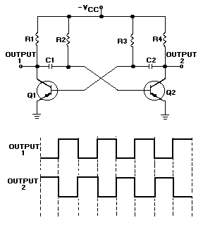
Figure 3-20. —Free-running multivibrator.
3-21
CLOCKS AND COUNTERS
Clocks and counters are found in all types of digital equipment. Although they provide different functions, they are all constructed of circuits with which you are familiar. By changing the way the circuits are interconnected, we can build timing circuits, multipliers and dividers, and storage units. In this section we will discuss the purpose, construction, and operation of these important digital circuits.
CLOCKS
Clocks have been mentioned in the preceding section with regard to their action with FFs. You will recall that the clock is a timing signal generated by the equipment to control operations. This control feature is demonstrated in both the D and J-K FFs. Remember that the clock output had to be in a certain condition for the FFs to perform their functions.
The simplest form of a clock is the astable or free-running multivibrator. A schematic diagram of a typical free-running multivibrator is shown in figure 3-20 along with its output waveforms. This multivibrator circuit is called free running because it alternates between two different output voltages during the time it is active. Outputs 1 and 2 will be equal and opposite since Q1 and Q2 conduct alternately. The frequency of the outputs may be altered within certain limits by varying the values of R2C1 and R3C2. You may want to review the operation of the astable multivibrator in NEETS, Module 9, Introduction to Wave-Generation and Wave-Shaping Circuits. Although the astable multivibrator circuit seems to produce a good, balanced square wave, it lacks the frequency stability necessary for some types of equipment.
The frequency stability of the astable multivibrator can be increased by applying a trigger pulse to the circuit. The frequency of the trigger must be higher than the free-running frequency of the multivibrator. The output frequency will match the trigger frequency and produce a more stable output.
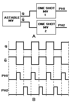
Figure 3-21. —Monostable multivibrator block diagram.
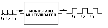
Figure 3-22. —Two-phase clock: A. Block diagram; B. Timing diagram.
3-22
Another method of producing a stable clock pulse is to use a triggered monostable or one-shot multivibrator. You will recall from NEETS, Module 9, that a one-shot multivibrator has one stable state and will only change states when acted on by an outside source (the trigger). A block diagram of a monostable multivibrator with input and output signals is shown in figure 3-21. The duration of the output pulse is dependent on the charge time of an RC network in the multivibrator. Each trigger input results in a complete cycle in the output, as shown in figure 3-21. Trigger pulses are supplied by an oscillator.
The circuits described previously are very simple clocks. However, as the complexity of the system increases, so do the timing requirements. Complex systems have multiphase clocks to control a variety of operations. Multiphase clocks allow functions involving more than one operation to be completed during a single clock cycle. They also permit an operation to extend over more than one clock cycle.
A block diagram of a two-phase clock system is shown in figure 3-22, view A. The astable multivibrator provides the basic timing for the circuit, while the one-shot multivibrators are used to shape the pulses. Outputs Q and Q are input to one-shot multivibrators 1 and 2, respectively. The resulting outputs are in phase with the inputs, but the duration of the pulse is greatly reduced as shown in view B.
3-23
Clocks are designed to provide the most efficient operation of the equipment. During the design phase, the frequency, pulse width, and the number of phases required is determined; and the clock circuit is built to meet those requirements.
Most modern high-speed equipment uses crystal-controlled oscillators as the basis for their timing networks. Crystals are stable even at extremely high frequencies.
Q33. What is a clock with regard to digital equipment? Q34. What is the simplest type of clock circuit? Q35. What is needed to use a monostable or one-shot multivibrator for a clock circuit? Q36. What type of clock is used when more than one operation is to be completed during one clock
cycle?
COUNTERS
A counter is simply a device that counts. Counters may be used to count operations, quantities, or periods of time. They may also be used for dividing frequencies, for addressing information in storage, or for temporary storage.
Counters are a series of FFs wired together to perform the type of counting desired. They will count up or down by ones, twos, or more.
The total number of counts or stable states a counter can indicate is called MODULUS. For instance, the modulus of a four-stage counter would be 1610, since it is capable of indicating 00002 to 11112. The term modulo is used to describe the count capability of counters; that is, modulo-16 for a four-stage binary counter, modulo-11 for a decade counter, modulo-8 for a three-stage binary counter, and so forth.
Ripple Counters
Ripple counters are so named because the count is like a chain reaction that ripples through the counter because of the time involved. This effect will become more evident with the explanation of the following circuit.
Figure 3-23, view A, shows a basic four-stage, or modulo-16, ripple counter. The inputs and outputs are shown in view B. The four J-K FFs are connected to perform a toggle function; which, you will recall, divides the input by 2. The HIGHs on the J and K inputs enable the FFs to toggle. The inverters on the clock inputs indicate that the FFs change state on the negative-going pulse.
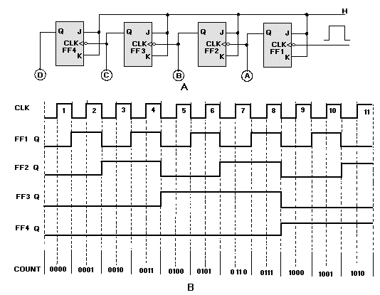
Figure 3-23. —Four-stage ripple counter: A. Logic diagram; B. Timing diagram.
3-24
Assume that A, B, C, and D are lamps and that all the FFs are reset. The lamps will all be out, and the count indicated will be 00002. The negative-going pulse of clock pulse 1 causes FF1 to set. This lights lamp A, and we have a count of 00012. The negative-going pulse of clock pulse 2 toggles FF1, causing it to reset. This negative-going input to FF2 causes it to set and causes B to light. The count after two clock pulses is 00102, or 210. Clock pulse 3 causes FF1 to set and lights lamp A. The setting of FF1 does not affect FF2, and lamp B stays lit. After three clock pulses, the indicated count is 00112.
Clock pulse 4 causes FF1 to reset, which causes FF2 to reset, which causes FF3 to set, giving us a count of 01002. This step shows the ripple effect.
This setting and resetting of the FFs will continue until all the FFs are set and all the lamps are lit. At that time the count will be 11112 or 1510. Clock pulse 16 will cause FF1 to reset and lamp A to go out. This will cause FF2 through FF4 to reset, in order, and will extinguish lamps B, C, and D. The counter would then start at 00012 on clock pulse 17. To display a count of 1610 or 100002, we would need to add another FF.
The ripple counter is also called an ASYNCHRONOUS counter. Asynchronous means that the events (setting and resetting of FFs) occur one after the other rather than all at once. Because the ripple count is asynchronous, it can produce erroneous indications when the clock speed is high. A high-speed clock can cause the lower stage FFs to change state before the upper stages have reacted to the previous clock pulse. The errors are produced by the FFs’ inability to keep up with the clock.
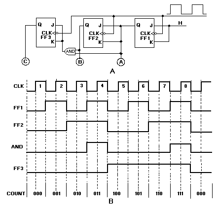
Figure 3-24. —Three-stage synchronous counter: A. Logic diagram; B. Timing Diagram.
3-25
Synchronous Counter
High-frequency operations require that all the FFs of a counter be triggered at the same time to prevent errors. We use a SYNCHRONOUS counter for this type of operation.
The synchronous counter is similar to a ripple counter with two exceptions: The clock pulses are applied to each FF, and additional gates are added to ensure that the FFs toggle in the proper sequence.
A logic diagram of a three-state (modulo-8) synchronous counter is shown in figure 3-24, view A. The clock input is wired to each of the FFs to prevent possible errors in the count. A HIGH is wired to the J and K inputs of FF1 to make the FF toggle. The output of FF1 is wired to the J and K inputs of FF2, one input of the AND gate, and indicator A. The output of FF2 is wired to the other input of the AND gate and indicator B. The AND output is connected to the J and K inputs of FF3. The C indicator is the only output of FF3.
During the explanation of this circuit, you should follow the logic diagram, view A, and the pulse sequences, view B.
Assume the following initial conditions: The outputs of all FFs, the clock, and the AND gate are 0; the J and K inputs to FF1 are HIGH. The negative-going portion of the clock pulse will be used throughout the explanation.
Clock pulse 1 causes FF1 to set. This HIGH lights lamp A, indicating a binary count of 001. The HIGH is also applied to the J and K inputs of FF2 and one input of the AND gate. Notice that FF2 and
3-26
FF3 are unaffected by the first clock pulse because the J and K inputs were LOW when the clock pulse was applied.
As clock pulse 2 goes LOW, FF1 resets, turning off lamp A. In turn, FF2 will set, lighting lamp B and showing a count of 0102. The HIGH from FF2 is also felt by the AND gate. The AND gate is not activated at this time because the signal from FF1 is now a LOW. A LOW is present on the J and K inputs of FF3, so it is not toggled by the clock.
Clock pulse 3 toggles FF1 again and lights lamp A. Since the J and K inputs to FF2 were LOW when pulse 3 occurred, FF2 does not toggle but remains set. Lamps A and B are lit, indicating a count of 0112. With both FF1 and FF2 set, HIGHs are input to both inputs of the AND gate, resulting in HIGHs to J and K of FF3. No change occurred in the output of FF3 on clock pulse 3 because the J and K inputs were LOW at the time.
Just before clock pulse 4 occurs, we have the following conditions: FF1 and FF2 are set, and the AND gate is outputting a HIGH to the J and K inputs of FF3. With these conditions all of the FFs will toggle with the next clock pulse.
At clock pulse 4, FF1 and FF2 are reset, and FF3 sets. The output of the AND gate goes to 0, and we have a count of 1002.
It appears that the clock pulse and the AND output both go to 0 at the same time, but the clock pulse arrives at FF3 before the AND gate goes LOW because of the transit time of the signal through FF1, FF2, and the AND gate.
Between pulses 4 and 8, FF3 remains set because the J and K inputs are LOW. FF1 and FF2 toggle in the same sequence as they did on clock pulses 1, 2, and 3.
Clock pulse 7 results in all of the FFs being set and the AND gate output being HIGH. Clock pulse 8 causes all the FFs to reset and all the lamps to turn off, indicating a count of 0002 . The next clock pulse (9) will restart the count sequence.
Q37. What is the modulus of a five-stage binary counter? Q38. An asynchronous counter is also called a ___________ counter. Q39. J-K FFs used in counters are wired to perform what function? Q40. What type of counter has clock pulses applied to all FFs? Q41. In figure 3-24, view A, what logic element enables FF3 to toggle with the clock? Q42. What is the largest count that can be indicated by a four-stage counter?
Decade Counter
A decade counter is a binary counter that is designed to count to 1010, or 10102. An ordinary four- stage counter can be easily modified to a decade counter by adding a NAND gate as shown in figure 3-25. Notice that FF2 and FF4 provide the inputs to the NAND gate. The NAND gate outputs are connected to the CLR input of each of the FFs.
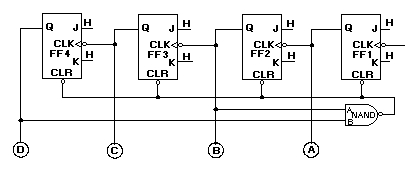
Figure 3-25. —Decade counter.
3-27
The counter operates as a normal counter until it reaches a count of 10102, or 1010. At that time, both inputs to the NAND gate are HIGH, and the output goes LOW. This LOW applied to the CLR input of the FFs causes them to reset to 0. Remember from the discussion of J-K FFs that CLR and PS or PR override any existing condition of the FF. Once the FFs are reset, the count may begin again. The following table shows the binary count and the inputs and outputs of the NAND gate for each count of the decade counter:
BINARY COUNT
NAND GATE INPUTS
NAND GATE OUTPUT
******* A B ******* 0000 0 0 1 0001 0 0 1 0010 1 0 1 0011 1 0 1 0100 0 0 1 0101 0 0 1 0110 1 0 1 0111 1 0 1 1000 0 1 1 1001 0 1 1 1010 1 1 0
Changing the inputs to the NAND gate can cause the maximum count to be changed. For instance, if FF4 and FF3 were wired to the NAND gate, the counter would count to 11002 (1210), and then reset.
Q43. How many stages are required for a decade counter? Q44. In figure 3-25, which two FFs must be HIGH to reset the counter?
Ring Counter
A ring counter is defined as a loop of bistable devices (flip-flops) interconnected in such a manner that only one of the devices may be in a specified state at one time. If the specified condition is HIGH,
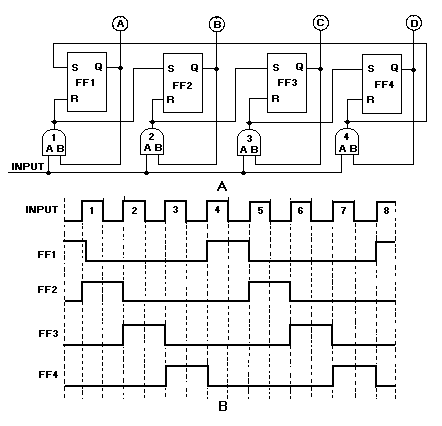
Figure 3-26. —Ring counter: A. Logic diagram; B. Timing diagram.
3-28
then only one device may be HIGH at one time. As the clock, or input, signal is received, the specified state will shift to the next device at a rate of 1 shift per clock, or input, pulse.
Figure 3-26, view A, shows a typical four-stage ring counter. This particular counter is composed of R-S FFs. J-K FFs may be used as well. Notice that the output of each AND gate is input to the R, or reset side, of the nearest FF and to the S, or set side, of the next FF. The Q output of each FF is applied to the B input of the AND gate that is connected to its own R input.
The circuit input may be normal CLK pulses or pulses from elsewhere in the equipment that would indicate some operation has been completed.
Now, let’s look at the circuit operation and observe the signal flow as shown in figure 3-26, view B.
For an initial condition, let’s assume that the output of FF1 is HIGH and that the input and FF2, FF3, and FF4 are LOW. Under these conditions, lamp A will be lit; and lamps B, C, and D will be extinguished. The HIGH from FF1 is also applied to the B input of AND gate 1.
The first input pulse is applied to the A input of each of the AND gates. The B inputs to AND gates 2, 3, and 4 are LOW since the outputs of FF2, FF3, and FF4 are LOW. AND gate 1 now has HIGHs on both inputs and produces a HIGH output. This HIGH simultaneously resets FF1 and sets FF2. Lamp A then goes out, and lamp B goes on. We now have a HIGH on AND gate 2 at the B input. We also have a LOW on AND gate 1 at input B.
3-29
Input pulse 2 will produce a HIGH output from AND gate 2 since AND gate 2 is the only one with HIGHs on both inputs. The HIGH from AND gate 2 causes FF2 to reset and FF3 to set. Indicator B goes out and C goes on.
Pulse 3 will cause AND gate 3 to go HIGH. This results in FF3 being reset and FF4 being set. Pulse 4 causes FF4 to reset and FF1 to set, bringing the counter full circle to the initial conditions. As long as the counter is operational, it will continue to light the lamps in sequence ¾ 1, 2, 3, 4; 1, 2, 3, 4, etc.
As we stated at the beginning of this section, only one FF may be in the specified condition at one time. The specified condition shifts one position with each input pulse.
Q45. In figure 3-26, view A, which AND gate causes FF3 to set? Q46. Which AND gate causes FF3 to reset? Q47. What causes the specified condition to shift position? Q48. If the specified state is OFF, how many FFs may be off at one time?
Down Counters
Up to this point the counters that you have learned about have been up counters (with the exception of the ring counter). An up counter starts at 0 and counts to a given number. This section will discuss DOWN counters, which start at a given number and count down to 0.
Up counters are sometimes called INCREMENT counters. Increment means to increase. Down counters are called DECREMENT counters. Decrement means to decrease.
A three-stage, ripple down counter is shown in figure 3-27, view A. Notice that the PS (preset) input of the J-K FFs is used in this circuit. HIGHs are applied to all the J and K inputs. This enables the FFs to toggle on the input pulses.
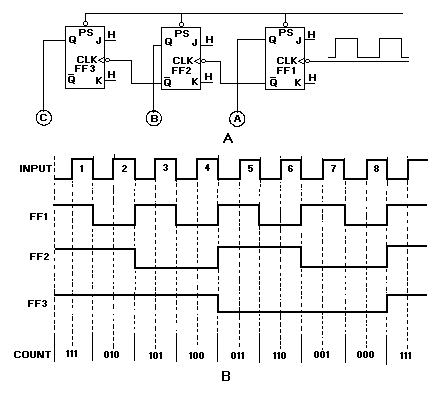
Figure 3-27. —Down counter: A. Logic diagram; B. Timing diagram.
3-30
A negative-going pulse is applied to all PS terminals to start the countdown. This causes all the FFs to set and also lights indicators A, B, and C. The beginning count is 1112 (710). At the same time, LOWs are applied to the CLK inputs of FF2 and FF3, but they do not toggle because the PS overrides any change. All actions in the counter will take place on the negative-going portion of the input pulse. Let’s go through the pulse sequences in figure 3-27, view B.
CP1 causes FF1 to toggle and output Q to go LOW. Lamp A is turned off. Notice that Q goes HIGH but no change occurs in FF2 or FF3. Lamps B and C are now on, A is off, and the indicated count is 1102 (610).
CP2 toggles FF1 again and lights lamp A. When Q goes HIGH, Q goes LOW. This negative-going signal causes FF2 to toggle and reset. Lamp B is turned off, and a HIGH is felt at the CLK input of FF3. The indicated count is 1012 (510); lamps A and C are on, and B is off.
At CP3, FF1 toggles and resets. Lamp A is turned off. A positive-going signal is applied to the CLK input of FF2. Lamp B remains off and C remains on. The count at this point is 1002 (410).
CP4 toggles FF1 and causes it to set, lighting lamp A. Now FF1, output Q , goes LOW causing FF2 to toggle. This causes FF2 to set and lights lamp B. Output of FF2, Q , then goes LOW, which causes FF3 to reset and turn off lamp C. The indicated count is now 0112 (310).
The next pulse, CP5, turns off lamp A but leaves B on. The count is now 0102. CP6 turns on lamp A and turns off lamp B, for a count of 0012. CP7 turns off lamp A. Now all the lamps are off, and the counter indicates 000.
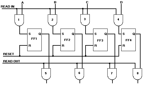
Figure 3-28. —Four-bit parallel register.
3-31
On the negative-going signal of CP8, all FFs are set, and all the lamps are lighted. The CLK pulse toggles FF1, making output Q go HIGH. As output Q goes LOW, the negative-going signal causes FF2 to toggle. As FF2, output Q, goes HIGH, output Q goes LOW, causing FF3 to toggle and set. As each FF sets, its indicator lamp lights. The counter is now ready to again start counting down from 1112 with the next CLK pulse.
Q49. How many FFs are required to count down from 1510? Q50. What signal causes FF2 to toggle?
REGISTERS
A register is a temporary storage device. Registers are used to store data, memory addresses, and operation codes. Registers are normally referred to by the number of stages they contain or by the number of bits they will store. For instance, an eight-stage register would be called an 8-bit register. The contents of the register is also called a WORD. The contents of an 8-bit register is an 8-bit word. The contents of a 4-bit register is a 4-bit word and so forth.
Registers are also used in the transfer of data to and from input and output devices such as teletypes, printers, and cathode-ray tubes.
Most registers are constructed of FFs and associated circuitry. They permit us to load or store data and to transfer the data at the proper time.
PARALLEL REGISTERS
Parallel registers are designed to receive or transfer all bits of data or information simultaneously.
A 4-bit parallel register is shown in figure 3-28. The data inputs are A, B, C, and D. The FFs store the data until it is needed. AND gates 5, 6, 7, and 8 are the transfer gates.
3-32
Before we go through the operation of the register, let’s set some initial conditions. Assume that inputs A, B, and D are HIGH and that FF2 and FF4 are set from a previous operation. The READ IN, READ OUT, and RESET inputs are all LOW.
To begin the operation, we apply a reset pulse to the RESET input of all the FFs, clearing the Q outputs to LOWs. This step ensures against any erroneous data transfer that would occur because of the states of FF2 and FF4.
Inputs A, B, C, and D are input to gates 1, 2, 3, and 4, respectively. When the READ IN input goes HIGH, AND gates 1, 2, and 4 go HIGH, causing FF1, FF2, and FF4 to set. The output of AND gate 3 does not change since the C input is LOW. The 4-bit word, 1101, is now stored in the register. The outputs of FFs 1, 2, 3, and 4 are applied to AND gates 5, 6, 7, and 8, respectively.
When the data is required for some other operation, a positive-going pulse is applied to the READ OUT inputs of the AND gates. This HIGH, along with the HIGHs from the FFs, causes the outputs of AND gates 5, 6, and 8 to go HIGH. Since the Q output of FF3 is LOW, the output of gate 7 will be LOW. The 4-bit word, 1101, is transferred to where it is needed.
Q51. How many stages are required to store a 16-bit word? Q52. Simultaneous transfer of data may be accomplished with what type of register? Q53. How are erroneous transfers of data prevented?
SHIFT REGISTERS
A shift register is a register in which the contents may be shifted one or more places to the left or right. This type of register is capable of performing a variety of functions. It may be used for serial-to- parallel conversion and for scaling binary numbers.
Before we get into the operation of the shift register, let’s discuss serial-to-parallel conversion, parallel-to-serial conversion, and scaling.
Serial and Parallel Transfers and Conversion
Serial and parallel are terms used to describe the method in which data or information is moved from one place to another. SERIAL TRANSFER means that the data is moved along a single line one bit at a time. A control pulse is required to move each bit. PARALLEL TRANSFER means that each bit of data is moved on its own line and that all bits transfer simultaneously as they did in the parallel register. A single control pulse is required to move all bits.
Figure 3-29 shows how both of these transfers occur. In each case, the four-bit word 1101 is being transferred to a storage device. In view A, the data moves along a single line. Each bit of the data will be stored by an individual control pulse. In view B, each bit has a separate input line. One control pulse will cause the entire word to be stored.
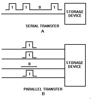
Figure 3-29. —Data transfer methods: A. Serial transfer; B. Parallel transfer.
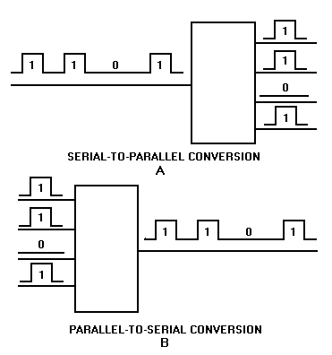
Figure 3-30. —Data conversion methods: A. Serial-to-parallel; B. Parallel-to-serial.
3-33
Serial-to-parallel conversion or parallel-to-serial conversion describes the manner in which data is stored in a storage device and the manner in which that data is removed from the storage device.
Serial-to-parallel conversion means that data is transferred into the storage device or register in serial fashion and removed in parallel fashion, as in figure 3-30, view A. Parallel-to-serial conversion means the data is transferred into the storage device in parallel and removed as serial data, as shown in view B.
Serial transfer takes time. The longer the word length, the longer the transfer will take. Although parallel transfer is much faster, it requires more circuitry to transfer the data.
3-34
Scaling
SCALING means to change the magnitude of a number. Shifting binary numbers to the left increases their value, and shifting to the right decreases their value. The increase or decrease in value is based on powers of 2.
A shift of one place to the left increases the value by a power of 2, which in effect is multiplying the number by 2. To demonstrate this, let’s assume that the following block diagram is a 5-bit shift register containing the binary number 01100.
0 1 1 0 0
Shifting the entire number one place to the left will put the register in the following condition:
1 1 0 0 0
The binary number 01100 has a decimal equivalent of 12. If we convert 110002 to decimal, we find it has a value of 2410. By shifting the number one place to the left, we have multiplied it by 2. A shift of two places to the left would be the equivalent of multiplying the number by 22, or 4; three places by 23, or 8; and so forth.
Shifting a binary number to the right decreases the value of the number by a power of 2 for each place. Let’s look at the same 5-bit register containing 011002 and shift the number to the right.
0 1 1 0 0
A shift of one place to the right will result in the register being in the following condition:
0 0 1 1 0
By comparing decimal equivalents you can see that we have decreased the value from 1210 to 610. We have effectively divided the number by 2. A shift of two places to the right is the equivalent of dividing the number by 22, or 4; three places by 23; or 8; and so forth.
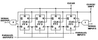
Figure 3-31. —Shift register.
3-35
Shift Register Operations
Figure 3-31shows a typical 4-bit shift register. This particular register is capable of left shifts only. There are provisions for serial and parallel input and serial and parallel output. Additional circuitry would be required to make right shifts possible.
Before any operation takes place, a CLEAR pulse is applied to the RESET terminal of each FF to ensure that the Q output is LOW.
The simplest modes of operation for this register are the parallel inputs and outputs. Parallel data is applied to the SET inputs of the FFs and results in either a 1 or 0 output, depending on the input. The outputs of the FFs may be sampled for parallel output. In this mode, the register functions just like the parallel register covered earlier in this section.
Parallel-to-Serial Conversion
Now let’s look at parallel-to-serial conversion. We will use the 4-bit shift register in figure 3-31 and the timing sequence in figure 3-32 to aid you in understanding the operations.
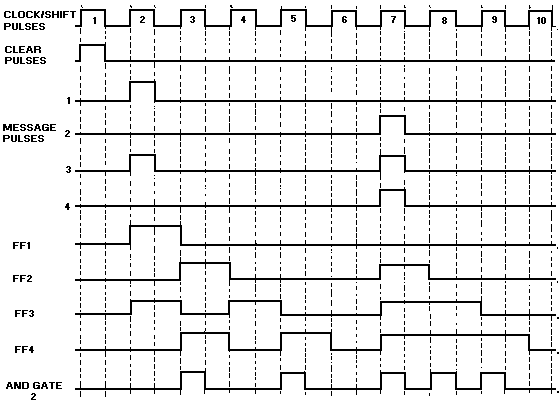
Figure 3-32. —Parallel-to-serial conversion timing diagram.
3-36
At CP1, a CLEAR pulse is applied to all the FFs, resetting the register to a count of 0. The number 01012 is applied to the parallel inputs at CP2, causing FF1 and FF3 to set. At this point, the J inputs of FF2 and FF4 are HIGH. AND gate 2 has a LOW output since the FF4 output is LOW. This LOW output represents the first digit of the number 01012 to be output in serial form. At the same time we have HIGHs on the K inputs of FF1 and FF3. (Notice the NOT symbol on FF1 at input K. With no serial input to AND gate 1, the output is LOW; therefore, the K input to FF1 is held HIGH). With these conditions CP3 causes FF1 and FF3 to reset and FF2 and FF4 to set. The HIGH output of FF4, along with CP3, causes AND gate 2 to output a HIGH. This represents the second digit of the number 01012.
At CP4, FF2 and FF4 reset, and FF3 sets. FF1 remains reset because of the HIGH at the K input. The output of AND gate 2 goes LOW because the output of FF4 is LOW and the third digit of the number is output on the serial line. CP5 causes FF4 to set and FF3 to reset. CP5 and the HIGH from FF4 cause AND gate 2 to output the last digit of the number on the serial line. It took a total of four CLK pulses to input the number in parallel and output it in serial.
CP6 causes FF4 to reset and effectively clears the register for the next parallel input.
Between CP7 and CP10, the number 11102 is input as parallel data and output as serial data.
Serial-to-Parallel Conversion
Serial input is accomplished much in the same manner as serial output. Instead of shifting the data out one bit at a time, we shift the data in one bit at a time.
To understand this conversion, you should again use figure 3-31and also the timing diagram shown in figure 3-33. In this example we will convert the number 10112 from serial data to parallel data.
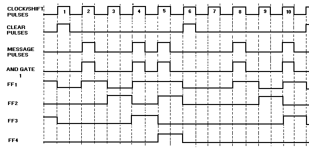
Figure 3-33. —Serial-to-parallel conversion timing diagram.
3-37
A CLEAR pulse resets all the FFs at CP1. At CP2, the most significant bit of the data is input to AND gate 1. This HIGH along with the clock pulse causes AND gate 1 to output a HIGH. The HIGH from the AND gate and the clock pulse applied to FF1 cause the FF to set. FFs 2, 3, and 4 are held reset. At this point, the MSD of the data has been shifted into the register.
The next bit of data is a 0. The output of AND gate 1 is LOW. Because of the inverter on the K input of FF1, the FF senses a HIGH at that input and resets. At the same time this is occurring, the HIGH on the J input of FF2 (from FF1) and the CLK cause FF2 to set. The two MSDs, 1 and 0, are now in the register.
CP4 causes FF3 to set and FF2 to reset. FF1 is set by the CLK pulse and the third bit of the number. The register now contains 01012, as a result of shifting the first three bits of data.
The remaining bit is shifted into the register by CP5. FF1 remains set, FF2 sets, FF3 resets, and FF4 sets. At this point, the serial transfer is complete. The binary word can be sampled on the parallel output lines. Once the parallel data is transferred, a CLEAR pulse resets the FFs (CP6), and the register is ready to input the next word.
Scaling Operation
Using the shift register shown in figure 3-31 for scaling a number is quite simple. The number to be scaled is loaded into the register either in serial or parallel form. Once the data is in the register, the scaling takes place in the same manner as that for shifting the data for serial output. A single clock pulse will cause each bit of data to shift one place to the left. Remember that each shift is the equivalent of increasing the value by a power of 2. The scaled data is read from the parallel outputs. Care must be taken not to over shift the data to the point that the MSDs are shifted out of the register.
Q54. Serial-to-parallel and parallel-to-serial conversions are accomplished by what type of circuit? Q55. What type of data transfer requires the most time? Q56. What is the main disadvantage of parallel transfer? Q57. How many FFs would be required for an 8-bit shift register?
3-38
Q58. How many clock pulses are required to output a 4-bit number in serial form? Q59. Two shifts to the left are equal to increasing the magnitude of a number by how much? Q60. To increase the magnitude of a number by 23, you must shift the number how many times and in
what direction?
LOGIC FAMILIES
Logic families are groups of logic circuits that are based on particular types of elements (resistors, transistors, and so forth). Families are identified by the manner in which the elements are connected, and, in some cases, by the types of elements used.
Logic circuits of a particular family can be interconnected without having to use additional circuitry. In other words, the output of one logic circuit can be used as the input to another logic circuit. This feature is known as compatibility. All circuits within a logic family will be compatible with the other circuits within that family.
As a technician, your responsibility will be to identify defective parts and repair or replace them as required. It will be beneficial for you to have a basic knowledge of the types of logic that are used in digital equipment.
Logic circuits are usually manufactured as integrated circuits and packaged in dual-inline packages (DIP), modified transistor outlines (TO), or flat packs. These packaging techniques are described in NEETS, Module 7, Introduction to Solid-State Devices and Power Supplies.
Circuitry in a package is normally shown using standard logic symbols instead of individual components such as transistors, diodes, and so forth. Figure 3-34 shows four examples of this type of packaging. The numbered blocks (1-14 and 1-16) are the pins on the package. Circuit packages are also identified by a manufacturer’s part number. Similar circuits produced by different manufacturers will not carry the same identification numbers in all cases.
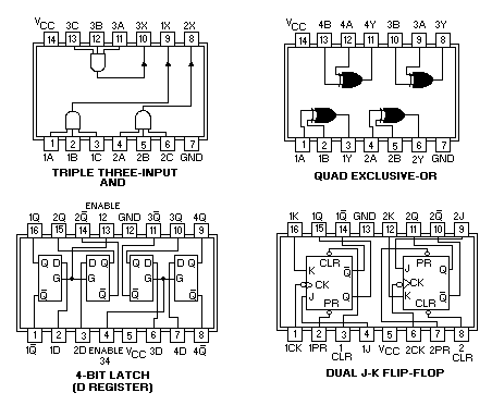
Figure 3-34. —Logic packages.
3-39
As mentioned before, logic families are identified by the elements used and the manner in which the elements are used. A brief description of some of the more common logic families follows.
RTL (RESISTOR-TRANSISTOR LOGIC) In this type of logic, inputs are applied to resistors, and the output is produced by a transistor. RTL is
normally constructed from discrete components (individual resistors and transistors). Some circuits are manufactured as integrated circuits and packaged in modified transistor outline (TO) packages, as shown in figure 3-35. An in-depth coverage of circuit packaging can be found in NEETS, Module 14, Introduction to Microelectronics.
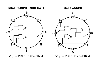
Figure 3-35. —RTL integrated circuits.
3-40
DTL (DIODE TRANSISTOR LOGIC) Input signals are applied to diodes in this logic family. The diodes either conduct or cut off and
produce the desired output from the transistor. DTL is normally found in dual-inline packages (DIP) as well as older discrete component logic.
TTL (TRANSISTOR-TRANSISTOR LOGIC) In TTL, transistors with multiple emitters are used for the logic inputs. Additional transistors are
used to produce the desired output. TTL is normally packed in DIPs and is quite common in military equipment.
CMOS (COMPLEMENTARY METAL OXIDE SEMICONDUCTORS) The CMOS logic circuits use metal oxide semiconductors similar to field-effect transistors (FETs).
LOGIC FAMILY USE
The logic family used in a piece of equipment is determined by the design engineers. The type of logic used will be based on the requirements of the equipment and on what family best fulfills the requirements.
The use of integrated circuits enables designers to produce equipment that is very small and highly efficient when compared to other methods of construction. The block diagram shown in figure 3-36, view A, represents an 8-bit, serial-input and parallel-output shift register. This circuit is contained in a standard 14-pin DIP measuring about 0.75 inch long and 0.25 inch wide. View B shows this circuit package.
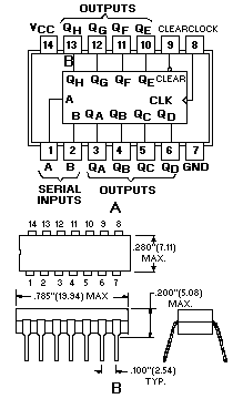
Figure 3-36. —Integrated logic circuits: A. Shift register; B. Logic package.
3-41
Q61. What are RTL, DTL, and TTL examples of? Q62. What type of logic family uses diodes in the input? Q63. What is the most common type of integrated circuit packaging found in military equipment? Q64. Circuits that can be interconnected without additional circuitry are known as ____________
circuits.
SUMMARY
Now that you have completed this chapter, you should have a basic understanding of the more common special logic circuits. The following is a summary of the emphasized terms and points found in the "Special Logic Circuits" chapter.
SPECIAL LOGIC CIRCUITS perform arithmetic and logic operations; input, output, store and transfer information; and provide proper timing for these operations.
EXCLUSIVE OR (X-OR) circuits produce a 1 output when ONLY one input is HIGH. Can be used as a quarter adder.
3-42
EXCLUSIVE NOR (X-NOR) circuits produce a 1 output when all inputs are 0 and when more than 1 input is 1.
QUARTER ADDER circuits produce the sum of two numbers but do not generate a carry. HALF ADDER circuits produce the sum of two numbers and generate a carry.
FULL ADDER circuits add a carry to obtain the correct sum.
PARALLEL ADDER circuits use full adders connected in parallel to accommodate the addition of multiple-digit numbers.
STANDARD SYMBOLS depict logic circuitry with blocks, showing only inputs and outputs. One block may contain many types of gates and circuits.
SUBTRACTION in binary is accomplished by complementing and adding.
FLIP-FLOP are bistable multivibrators used for storage, timing, arithmetic operations, and transfer of information.
R-S FFs have the Q output of the FF HIGH in the set mode and LOW in the reset mode.
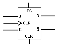
3-43
T (TOGGLE) FFS change state with each pulse applied to the input. Each T FF will divide the input by 2.
D FF is used to store data at a predetermined time.
J-K FF is the most versatile FF. J-Ks can perform the same functions as all the other FFs.
CLOCKS are circuits that generate the timing and control signals for other operations.
COUNTERS are used to count operations, quantities, or periods of time. They can be used to divide frequencies, to address information in storage, or as temporary storage.
MODULUS of a counter is the total number of counts or stable states a counter may indicate.
UP COUNTERS count from 0 to a predetermined number.
DOWN COUNTERS count from a predetermined number to 0.
RING COUNTERS are loop counters that may be used for timing operations.
REGISTERS are used as temporary storage devices as well as for transfer of information.
PARALLEL REGISTERS receive or transfer all bits of data simultaneously.
SHIFT REGISTERS are used to perform serial-to-parallel and parallel-to-serial conversion and for scaling binary numbers.
3-44
SERIAL TRANSFER causes all bits of data to be transferred on a single line.
PARALLEL TRANSFER has each data bit on its own line.
SCALING of binary numbers means to increase or decrease the magnitude of a number by a power of 2.
LOGIC FAMILIES are composed of logic circuits based on particular types of elements.
ANSWERS TO QUESTIONS Q1. THROUGH Q64. A1. ¯ .
A2. Low (0). A3. One or the other of the inputs must be HIGH, but not both at the same time. A4. Exclusive NOR (X-NOR). A5. HIGH.
A6. The half adder generates a carry. A7. Quarter adder. A8. Sum equals 0 with a carry of 1. A9. Full adder.
A10. Four.
A11. S1 = 1, S2 = 0 and C2 = 1.
A12. C1 = 0.
A13. X-OR gates.
A14. Four.
A15. MSD of the sum. A16. Add 1 portion.
A17. Subtrahend.
A18. Storing information. A19. Six.
A20. 1 and 0, or opposite states.
A21. By cross-coupling NAND or OR gates.
A22. One.
3-45
A23. To divide the input by 2.
A24. Clock and data.
A25. Up to one clock pulse.
A26. A positive-going clock pulse.
A27. J-K flip-flop. A28. Set, or HIGH (1). A29. When the clock pulse goes LOW.
A30. Both J and K must be HIGH.
A31. Clear (CLR) and preset (PS or PR). A32. The flip-flop is jammed. A33. A timing signal.
A34. An astable or free-running multivibrator. A35. Triggers.
A36. A multiphase clock.
A37. 32.
A38. Ripple.
A39. Toggle.
A40. Synchronous.
A41. The AND gate.
A42. 11112, or 1510.
A43. Four.
A44. FFs 2 and 4.
A45. Two.
A46. Three.
A47. The input, or clock pulse.
A48. One.
A49. Four.
A50. Q output of FF 1 going LOW.
3-46
A51. 16.
A52. Parallel.
A53. By clearing the register.
A54. Shift register. A55. Serial.
A56. Requires more circuitry.
A57. Eight.
A58. Four.
A59. 22, or four times. A60. Three to the left. A61. Logic families. A62. DTL (diode transistor logic). A63. DIPs (dual inline packages). A64. Compatible.
AI-1
APPENDIX I
GLOSSARY
ADDEND ¾ A number to be added to an augend.
ADDITION ¾ A form of counting where on quantity is added to another.
AND GATE ¾ A logic circuit in which all inputs must be HIGH to produce a HIGH output.
ASSOCIATIVE LAW ¾ A simple equality statement A(BC) = ABC or A+(B+C) = A+B+C.
AUGEND ¾ A number to which another number is to be added.
BASE ¾ The number of symbols used in the particular number system.
BCD (BINARY CODED DECIMAL) ¾ A method of using binary digits to represent the decimal digits 0 through 9.
BINARY SYSTEM ¾ The base 2 number system using 0 and 1 as the symbols.
BOOLEAN ALGEBRA ¾ A mathematical concept based on the assumption that most quantities have two possible conditions ¾ TRUE and FALSE.
BOOLEAN EXPRESSION ¾ A description of the input or output conditions of a logic gate.
BORROW ¾ To transfer a digit (equal to the base of the number system) from the next higher order column for the purpose of subtraction.
CARRY ¾ A carry is produced when the sum of two or more numbers in a vertical column equals or exceeds the base of the number system in use.
CLOCK ¾ A circuit that generates timing control signals in a computer or other type of digital equipment.
COMMUTATIVE LAW ¾ The order in which terms are written does not affect their value; AB = BA, A+B = B+A.
COMPATIBILITY ¾ The feature of logic families that allows interconnection of circuits without the need for additional circuitry.
COMPLEMENT ¾ Something used to complete something else.
COMPLEMENTARY LAW ¾ A term ANDed with its complement is 0, and a term ORed with its complement is 1; A A = 0, A + A = 1.
CONVERSION ¾ To change a number in one base to its equivalent in another base.
COUNTER ¾ A device that counts.
D FLIP-FLOP ¾ Stores the data bit (D) in conjunction with the clock input. DECADE COUNTER ¾ Counter from 0 to 1010 in base 2, then resets.
DECIMAL POINT ¾ The radix point for the decimal system.
AI-2
DECIMAL SYSTEM ¾ A number system with a base or radix of 10.
DEMORGAN’S THEOREM ¾ This theorem has two parts: the first states that AB = A + B ; the second states that BA + = A B .
DIFFERENCE ¾ That which is left after subtraction.
DISTRIBUTIVE LAW ¾ (1) a term (A) ANDed with a parenthetical expression (B+C) equals that term ANDed with each term within the parenthesis: A(B+C) = AB+AC; (2) a term (A) ORed with a parenthetical expression (BC) equals that term ORed with each term within the parenthesis: A+(BC) = (A+B)(A+C).
DIVIDEND ¾ A number to be divided.
DIVISOR ¾ A number by which a dividend is divided.
DOUBLE NEGATIVE LAW ¾ A term that is inverted twice is equal to the term; A = A.
DOWN COUNTER¾ A circuit that counts from a predetermined number down to 0.
EXCLUSIVE-NOR (X-NOR) ¾ A logic circuit that produces a HIGH output when all inputs are LOW or all inputs are HIGH.
EXCLUSIVE-OR (X-OR) GATE ¾ A logic circuit that produces a HIGH output when one and only one input is HIGH.
EXPONENT ¾ A number above and to the right of a base indicating the number of time the base is multiplied by itself; 24 = 2 · 2 · 2 · 2.
FLIP-FLOP ¾ A bistable multivibrator.
FRACTIONAL NUMBER ¾ A symbol to the right of the radix point that represents a portion of a complete object.
HEXADECIMAL (HEX) SYSTEM ¾ The base 16 number system using 0 through 9 and A, B, C, D, E, and F as symbols.
IDEMPOTENT LAW ¾ States that a term ANDed with itself or ORed with itself is equal to the term; AA = A, A+A = A.
INVERTER ¾ A logic gate that outputs the complement of its input.
J-K FLIP-FLOP ¾ Can perform the functions of the RS, T, and D flip-flops.
LAW OF ABSORPTION ¾ This law is the result of the application of several other laws. It states that A(A+B) = A or A+(AB) = A.
LAW OF COMMON IDENTITIES ¾ The two statements A( A +B) = AB and A+ A B = A+B are based on the complementary law.
LAW OF IDENTITY ¾ States that a term TRUE in one part of an expression will be TRUE in all parts of the expression; A = A, A = A .
LAW OF INTERSECTION ¾ A term ANDed with 1 equals that term, and a term ANDed with 0 equals 0; A·1 = A, A· 0 = 0.
AI-3
LAW OF UNION ¾ A term ORed with 1 equals 1; a term ORed with 0 equals that term; A+1 = 1, A + 0 = 0.
LEAST SIGNIFICANT (LSD) ¾ The digit which has the least effect on the value of a number.
LOGIC ¾ The science of reasoning; the development of a reasonable or logical conclusion based on known information.
LOGIC FAMILY ¾ A group of logic circuits based on specific types of circuit elements (DTL, TTL, CMOS, and so forth).
LOGIC GATES ¾ Decision-making circuits in computers and other types of equipment.
LOGIC POLARITY ¾ The polarity of a voltage used to represent the logic 1 state.
LOGIC SYMBOL ¾ Standard symbol used to indicate a particular logic function.
MINUEND ¾ The number from which another number is subtracted.
MIXED NUMBER ¾ Represents one or more complete units and a portion of a single unit.
MODULUS ¾ The number of different values that a counter can contain or display.
MOST SIGNIFICANT DIGIT (MSD) ¾ The digit which if changed will have the greatest effect on the value of a number.
NAND GATE ¾ An AND gate with an inverted output. The output is LOW when all inputs are HIGH, and HIGH when any or all inputs are LOW.
NEGATIVE LOGIC ¾ The voltage representing logic state 1 is more negative that the voltage representing a logic state 0.
NEGATOR ¾ See inverter.
NOR GATE ¾ An OR gate with an inverted output. The output is LOW when any or all inputs are HIGH, and HIGH when all inputs are LOW.
NOT CIRCUIT ¾ See inverter.
NUMBER ¾ A symbol used to represent a unit or a quantity.
OCTAL SYSTEM ¾ The base 8 number system using 0 through 7 as the symbols.
OR GATE ¾ A logic circuit which produces a HIGH output when one or more inputs is/are HIGH.
PARALLEL DATA ¾ Each bit of data has a separate line and all bits are moved simultaneously.
PARALLEL REGISTER ¾ A register that receives, stores, and transfers data in a parallel mode.
POSITIONAL NOTATION ¾ A method where the value of the number is defined by the symbol and the symbol’s position.
POSITIVE LOGIC ¾ The voltage representing logic state 1 is more positive than the voltage representing a logic state 0.
POWER OF A NUMBER ¾ The number of times a base is multiplied by itself. The power of a base is indicated by the exponent; that is, 103 = 10 · 10 · 10.
AI-4
QUOTIENT ¾ The result in division.
RADIX POINT ¾ The symbol that separates whole numbers and fractional numbers.
RADIX ¾ The total number of symbols used in a particular number system.
REGISTER ¾ A circuit of flip-flops designed to receive, store, and transfer data.
REMAINDER ¾ The final undivided part that is less than the divisor.
RING COUNTER ¾ A loop in which only one flip-flop will be set at any given time; used in timing.
RIPPLE (ASYNCHRONOUS) COUNTER ¾ A circuit that counts from 0 to a specified value. Subject to error at high frequency.
R’s (RADIX) COMPLEMENT ¾ The difference between a given number and the next higher power of the number system (10008 minus 2548 equals 5248).
R’s-1 (RADIX-1) COMPLEMENT ¾ The difference between a given number and the highest value symbol in the number system (7778 minus 2548 equals 5248).
R-S FLIP-FLOP ¾ A flip-flop with two inputs ¾ S (set) and R (reset). The Q output is HIGH in the set mode and LOW in the reset mode.
SERIAL DATA ¾ All data bits are transferred one bit at a time along a single conductor.
SHIFT REGISTER ¾ A register capable of serial-to-parallel and parallel-to-serial conversion and scaling.
SHIFTING ¾ Moving the contents of a register right or left to scale the number or to input or output serial data.
SUBSCRIPT ¾ A number written below and to the right of a value indicating the base or radix of the number system in use (358).
SUBTRACTION ¾ Taking away one number from another.
SUBTRAHEND ¾ The quantity to be subtracted from the minuend.
SUM ¾ The result in addition.
SYNCHRONOUS COUNTER ¾ Performs the same function as a ripple counter but error free at high frequency.
T FLIP-FLOP ¾ A single input flip-flop that changes state with each positive pulse or each negative pulse. Divides input frequency by two.
TRUTH TABLE ¾ A chart showing all possible input combinations and the resultant outputs.
UNIT ¾ A single object. UP/DOWN COUNTER ¾ A counter circuit that can count up or down on command.
VINCULUM ¾ A bar over a logic statement indicating the FALSE condition of the statement.
WHOLE NUMBER ¾ A symbol that represents one or more complete objects. ZERO ¾ A symbol that indicates no numerical value for a position in positional notation.
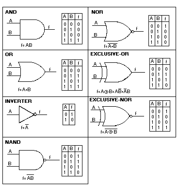
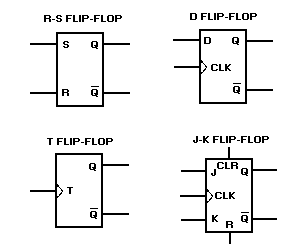
INDEX-1
MODULE 13 INDEX A Adders, 3-5 Addition, 1-6, 1-7
binary numbers, 1-8 hex numbers, 1-29 to 1-38 octal numbers, 1-24 to 1-31
AND gate, 2-6 AND/NAND gate variations, 2-18 B Background and history, number systems, 1-2,
1-3 Base (radix), 1-3, 1-9, 1-24, 1-30 Binary coded decimal, 1-56
BCD addition, 1-57 BCD conversion, 1-57
Binary conversion, 1-46 binary to decimal, 1-51 binary to hex, 1-47 binary to octal, 1-46
Binary number systems, 1-8 Boolean algebra, 2-28 Borrow and carry principles, 1-6 C Carry and borrow principles, 1-6 Clocks and counters, 3-22 CMOS (complementary metal oxide
semiconductors), 3-41 Complementary subtraction, 1-18, 3-11 Computer logic, 2-1 Conversion of bases, 1-37 Conversion to decimal, 1-51
binary to decimal, 1-51 hex to decimal, 1-55 octal to decimal, 1-53
D D flip-flop, 3-7 Decade counter, 3-27
Decimal conversion, 1-37 decimal to binary, 1-37 decimal to hex, 1-44 decimal to octal, 1-41
Decimal number system, 1-2 Down counters, 3-30 DTL (diode transistor logic), 3-41 E Exclusive NOR gate, 3-4 Exclusive OR gate, 3-3 F Flip-flops, 3-12 Full adder, 3-7 Fundamental logic circuits, 2-1
AND gate, 2-6 Boolean algebra, 2-28 computer logic, 2-1 introduction, 2-1 inverter (NOT gate), 2-12 logic gates in combination , 2-23 NAND gate, 2-14 NOR gate, 2-16 OR gate, 2-10 summary, 2-32 variations of fundamental gates, 2-18
G General logic, 2-1 Glossary, AI-1 to AI-4 H Half-adder, 3-6 Hex conversion, 1-50
hex to binary, 1-51 hex to decimal, 1-55 hex to octal, 1-51
INDEX-2
Hexadecimal (hex) number system, 1-29
I Inverter (NOT gate), 2-12 J J-K flip-flop, 3-18 L Laws and theorems, 2-30 Learning objectives, 1-1, 2-1, 3-1 Logic conditions, 2-2 Logic families, 3-39 Logic families use, 3-40 Logic gates in combination, 2-23 Logic inputs and outputs, 2-4 Logic levels, 2-2 Logic states, 2-2 Logic symbol, 2-6, 2-11, 2-14, 2-16
AND gate, 2-6 NAND gate, 2-14 NOR gate, 2-16 OR gate, 2-10
Logic symbols, AII-1 to AII-2 M Modern use, number systems, 1-2 Most significant digit (MSD) and least
significant digit (LSD), 1-5, 1-11, 1-24, 1-31 N NAND gate, 2-14 Negative and positive logic, 2-3 NOR gate, 2-16 Number systems, 1-2
conversion of bases, 1-37 introduction, 1-1 summary, 1-59 types of number systems, 1-2
O Octal conversion, 1-49
octal to binary, 1-49 octal to decimal, 1-53 octal to hex, 1-50
Octal numbers, 1-22 Operations, 2-6, 2-10, 2-15, 2-17
AND gate, 2-6 NAND gate, 2-14 NOR gate, 2-16 OR gate, 2-10
OR gate, 2-10 OR/NOR gate variations, 2-20 P Parallel adders, 3-8 Parallel registers, 3-32 Parallel-to-serial conversion, 3-36 Positional notation, 1-9, 1-23, 1-30 Positional notation and zero, 1-3 Positive and negative logic, 2-3 Q Quarter adder, 3-5 R Radix (base), 1-3, 1-9, 1-23, 1-30 Registers, 3-32 Ring counter, 3-28 Ripple counters, 3-24 R-S flip-flop, 3-13 RTL (resistor-transistor logic), 3-40 S Scaling, 3-35 Scaling operation, 3-38 Serial and parallel transfers and conversion,
3-33 Serial-to-parallel conversion, 3-37 Shift register operations, 3-36 Shift registers, 3-33
INDEX-3
Special logic circuits, 3-1 adders, 3-5 clocks and counters, 3-22 exclusive NOR gate, 3-4 exclusive OR gate, 3-3 flip-flops, 3-12 introduction, 3-1 logic families, 3-39 registers, 3-32 summary, 3-42
Subtraction, 3-11 binary numbers, 1-16 hex numbers, 1-34 octal numbers, 1-27
Synchronous counter, 3-26 T Toggle flip-flop, 3-16
Truth Table, 2-7, 2-11, 2-16, 2-17 AND gate, 2-6 NAND gate, 2-14 NOR gate, 2-16 OR gate, 2-10
TTL (transistor-transistor logic), 3-41 Types of number systems, 1-2 U Unit and number, 1-3, 1-9, 1-23, 1-30 V Variations of fundamental gates, 2-18 Z Zero and positional notation, 1-3
Assignment Questions
Information: The text pages that you are to study are provided at the beginning of the assignment questions.
1
ASSIGNMENT 1
Textbook Assignment: "Number Systems," chapter 1, pages 1-1 through 1-69. _________________________________________________________________________________
1-1. Modern number systems are built around which of the following components?
1. Unit, number, and radix 2. Number, base, and radix 3. Position, power, and unit 4. Digit, power, and position
1-2. What term describes a single object in a modern number system?
1. Unit 2. Base 3. Digit 4. Number
1-3. What is a number?
1. A quantity of objects 2. A counting system based on symbols 3. The decimal system 4. A symbol representing a unit or a
quantity
1-4. Which of the following symbols is NOT an Arabic figure?
1. C 2. 2 3. 7 4. 9
1-5. What term describes the number of symbols used in a number system?
1. Power 2. Radix 3. Exponent 4. Subscript
1-6. What is the base of a number system using all the letters of the alphabet ¾ A=0, B=1, C=2, and so forth?
1. 29 2. 25 3. 28 4. 26
1-7. A number system uses the symbols 0 through 4. What is its base?
1. 6 2. 5 3. 3 4. 4
1-8. Using positional notation, what two factors determine the value of a number?
1. Symbol and position 2. Position and base 3. Radix and symbol 4. Unit and symbol
1-9. How many decimal units are represented by the 5 in the number 157210?
1. 100 2. 50 3. 500 4. 5000
1-10. The 1 in 157210 is equal to what power of ten?
1. 101 2. 102 3. 103 4. 104
2
1-11. The power of a number is indicated by the
1. subscript 2. exponent 3. radical 4. radix
1-12. What is the value of 5 times 100?
1. 1 2. 0.5 3. 5 4. 50
1-13. Which of the following numbers is a mixed number?
1. 14.03 2. 156 3. 1,257 4. .0004
1-14. What term describes the symbol that separates the whole and fractional numbers in any number system?
1. Exponent 2. Radix point 3. Decimal point 4. Position point
1-15. What is the MSD of (a) 0.4201, (b) 13, and (c) 32.06?
1. (a) 4 (b) 1 (c) 3 2. (a) 1 (b) 3 (c) 2 3. (a) 2 (b) 1 (c) 2 4. (a) 4 (b) 3 (c) 3
1-16. What term is defined as a number to be added to a preceding number?
1. Addend 2. Augend 3. Carry 4. Sum
1-17. Identify A through D in the following example.
1 – A 25 – B + 17 – C 42 – D
1. Addend, sum, carry, augend 2. Carry, augend, addend, sum 3. Augend, carry, sum, addend 4. Carry, augend, sum, addend
IN ANSWERING QUESTION 1-18, PERFORM THE INDICATED OPERATION.
1-18. Add:
1. 418 2. 508 3. 528 4. 518
1-19. In subtraction, the (a) is subtracted from the (b).
1. (a) Minuend (b) subtrahend 2. (a) Remainder (b) subtrahend 3. (a) Subtrahend (b) difference 4. (a) Subtrahend (b) minuend
1-20. A borrow is required in which of the following examples?
1.
2.
3.
4.
3
1-21. The result of subtraction is known as the
1. addend 2. quotient 3. difference 4. subtrahend
1-22. What are the (a) radix and (b) the symbols used in the binary number system?
1. (a) 1 (b) 0, 1 2. (a) 2 (b) 1, 0 3. (a) 3 (b) 0, 1, 2 4. (a) 0 (b) 1, 2
1-23. Positional notation for the binary system is based on powers of
1. 1 2. 2 3. 3 4. 0
1-24. What is the decimal equivalent of 23?
1. 6 2. 2 3. 8 4. 10
1-25. The decimal number 1 is equal to what power of two?
1. 21 2. 22 3. 23 4. 20
1-26. Which of the following powers of two indicates a fraction?
1. 21 2. 20 3. 2 - 2 4. 22
1-27. Which digit is the MSD in the binary number 1011001?
1. The 0 farthest to the left 2. The 1 farthest to the left 3. The 0 farthest to the right 4. The 1 farthest to the right
1-28. Which of the following combinations of binary addition is INCORRECT?
1. 1 + 1 = 1 with a carry 2. 1 + 0 = 1 3. 0 + 0 = 0 4. 0 + 1 = 1
IN ANSWERING QUESTIONS 1-29 THROUGH 1-33, PERFORM THE INDICATED OPERATION.
1-29. Add:
100102
+ 10102
1. 100002 2. 111002 3. 101012 4. 110102
1-30. Add:
111012
+ 010012
1. 111112 2. 1001102 3. 1110102 4. 1000002
4
1-31. Add:
1112 + 0012
1. 1002 2. 10102 3. 10012 4. 10002
1-32. Add:
1002 0102 + 0012
1. 10002 2. 10012 3. 1012 4. 1112
1-33. Add:
110102 1002 + 1112
1. 0111102 2. 1010102 3. 100101 4. 1110012
1-34. Which of the following rules of binary subtraction is correct?
1. 0 - 0 = 0 with a borrow 2. 1 - 0 = 0 3. 2 - 1 = 1 4. 1 - 0 = 1
1-35. In the following example, which number is the minuend?
101102 – 11002
1. 101102 2. 11002 3. 10102 4. 101012
1-36. Which of the following rules of binary subtraction requires the use of a borrow?
1. 0 - 0 2. 1 - 0 3. 1 - 1 4. 0 - 1
1-37. In binary subtraction, what is the value of a borrow when it is moved to the next lower order column?
1. 12 2. 22 3. 102 4. 1010
IN ANSWERING QUESTIONS 1-38 THROUGH 1-40, PERFORM THE INDICATED OPERATION.
1-38. Subtract:
111112 – 101012
1. 101002 2. 110102 3. 001012 4. 010102
1-39. Subtract:
101012 – 11112
1. 001102 2. 010012 3. 011002 4. 000102
5
1-40. Subtract:
100012 – 01102
1. 10102 2. 10112 3. 11102 4. 10012
1-41. Subtraction is accomplished by which of the following methods in a computer that can only add?
1. Binary subtraction 2. Decimal complement 3. Complementary subtraction 4. Minuend complement
1-42. What is the R's-1 complement of 63310?
1. 47710 2. 46610 3. 36610 4. 37710
1-43. What is the R's-1 complement of 10111012?
1. 01000102 2. 10111102 3. 898889810 4. 898889910
1-44. What is the R's complement of 39510?
1. 60410 2. 60510 3. 71510 4. 71410
1-45. Which of the following parts of a subtraction problem must be complemented to perform complementary subtraction?
1. Subtrahend 2. Difference 3. Remainder 4. Minuend
1-46. Which of the following examples is the correct step when using the R's complement to subtract 12310 from 26410?
1. 735 + 123
2. 264 + 876
3. 264 + 321
4. 264 + 877
1-47. Which of the following solutions is correct when using the R's complement method of subtracting 51610 from 84510?
1. 845 + 483 328
2. 845 + 484 329
3. 845 + 615 460
4. 155 + 516 671
1-48. Which of the following numbers is the R's-1 complement of the binary number 10101?
1. 101002 2. 010112 3. 011002 4. 010102
6
1-49. Perform the R’s-1 complement of the following binary numbers.
(a) 1000, (b) 1101, (c) 0100
1. (a) 01112 (b) 00102 (c) 10112 2. (a) 01102 (b) 00112 (c) 10102 3. (a) 01112 (b) 00112 (c) 10112 4. (a) 01102 (b) 00102 (c) 10102
1-50. Which of the following statements regarding the forming of the R’s complement of a binary number is correct?
1. Retain the MSD and complement all other digits
2. Complement all digits and subtract 1 3. Complement all digits 4. Retain the least significant 1 and
complement all other digits to the left
1-51. Which of the following numbers is the R’s complement of 1001012?
1. 1010102 2. 0110112 3. 1101102 4. 1010012
IN ANSWERING QUESTIONS 1-52 AND 1-53, USE THE R’S COMPLEMENT METHOD TO SOLVE THE PROBLEMS.
1-52. Subtract:
10012 - 1012
1. 1102 2. 0102 3. 1002 4. 11002
1-53. Subtract:
11012 - 10102
1. 00012 2. 01002 3. 01102 4. 00112
1-54. In the previous problems, what is indicated by the carry that expands the difference by one place?
1. The answer is incorrect 2. The answer is a positive number 3. The answer is correct 4. The answer is a negative number
IN ANSWERING QUESTIONS 1-55 THROUGH 1-57, SOLVE THE SUBTRACTION PROBLEMS AND INDICATE THE SIGN OF THE DIFFERENCE.
1-55. Subtract:
100102 - 100012
1. 000012 positive 2. 011112 negative 3. 011002 positive 4. 000012 negative
1-56. Subtract:
00012 - 11112
1. 00102 negative 2. 01112 positive 3. 11102 negative 4. 11112 positive
7
1-57. Subtract:
011112 - 100002
1. 111112 negative 2. 000012 negative 3. 011112 positive 4. 100002 positive
1-58. What is the radix of the octal number system?
1. 1010 2. 0 to 7 3. 8 4. 78
1-59. Which of the following is NOT a valid octal number?
1. 6048 2. 5918 3. 7438 4. 4778
1-60. Which of the following equations is correct?
1. 80 = 8 2. 81 = 1 3. 84 = 8 · 8 · 8 4. 82 = 8 · 8
1-61. One octal digit is represented by how many binary digits?
1. One 2. Two 3. Three 4. Four
1-62. What is the decimal value of 83?
1. 6410 2. 12810 3. 25610 4. 51210
1-63. Which of the following symbols is the least significant digit of the octal number 1622.374?
1. 1 2. 2 3. 6 4. 4
1-64. What is the sum of 48 and 48?
1. 1010 2. 108 3. 78 4. 168
1-65. What is the sum of 778 and 38?
1. 1278 2. 808 3. 1008 4. 1028
IN ANSWERING QUESTION 1-66, PERFORM THE INDICATED OPERATION.
1-66. Add:
3748 + 1658
1. 4658 2. 5618 3. 4378 4. 5318
1-67. Find the sum of 77418 and 678.
1. 100008 2. 100308 3. 70308 4. 107308
1-68. What is the sum of 78, 68, 58, and 48?
1. 228 2. 178 3. 268 4. 248
8
IN ANSWERING QUESTIONS 1-69 AND 1-70, PERFORM THE INDICATED OPERATION.
1-69. Add:
26018 + 50358
1. 76368 2. 76408 3. 106368 4. 107008
1-70. Add:
23458 + 76548
1. 101108 2. 107418 3. 105718 4. 122218
1-71. Which, if any, of the following is a difference between subtracting octal numbers and subtracting decimal numbers?
1. The amount of the borrow 2. The octal minuend is converted to
decimal 3. The octal subtrahend is converted to
decimal 4. None; there is no difference
IN ANSWERING QUESTIONS 1-72 THROUGH 1-74, PERFORM THE INDICATED OPERATION.
1-72. Subtract:
6468 – 4218
1. 1258 2. 2658 3. 2258 4. 22510
1-73. Subtract:
4218 – 2678
1. 1448 2. 2328 3. 1328 4. 1428
1-74. Subtract:
30008 - 7778
1. 20018 2. 20118 3. 21118 4. 20008
9
ASSIGNMENT 2 Textbook assignment: Chapter 2, “Number Systems,” pages 2-1 through 2-36.
_____________________________________________________________________________________
2-1. Which of the following numbers does NOT represent a hexadecimal value?
1. 2DF4 2. A32B 3. 47CE 4. 9FGF
2-2. What is the decimal value of the highest symbol in the hex system?
1. 1510 2. 1610 3. F16 4. 1016
2-3. The decimal number 256 is equal to what power of 16?
1. 163 2. 162 3. 164 4. 161
2-4. List the MSD and LSD of the hex number F24.ECB.
1. MSD = 4, LSD = E 2. MSD = 4, LSD = B 3. MSD = F, LSD = 4 4. MSD = F, LSD = B
IN ANSWERING QUESTIONS 2-5 THROUGH 2-7, PERFORM THE INDICATED OPERATION.
2-5. Find the sum.
A16 + 416
1. C16 2. D16 3. E16 4. F16
2-6. Add:
1E16 + 1916
1. 3316 2. 3116 3. 3716 4. 4716
2-7. Add:
47816 +79216
1. C1116 2. C0A16 3. B0016 4. BFA16
2-8. When a borrow is taken from a hex number, that number is reduced by how much?
1. 1 2. 1016 3. 1610 4. 1010
10
IN ANSWERING QUESTION 2-9, FIND THE DIFFERENCE.
2-9. Subtract:
1016 – 816
1. A16 2. 716 3. 816 4. 916
2-10. To begin conversion of a decimal number to a different base, divide the (a) by (b).
1. (a) new base (b) 10
2. (a) decimal number (b) 2
3. (a) decimal number (b) the new base
4. (a) new base (b) the decimal equivalent
2-11. Which of the following terms describes the first remainder when converting decimal numbers to other bases?
1. MSD 2. LSD 3. Radix of the new base 4. Exponent of the new base
IN ANSWERING QUESTIONS 2-12 THROUGH 2-14, USE THE DIVISION METHOD TO CONVERT DECIMAL NUMBERS TO BINARY.
2-12. 4310
1. 1010112 2. 1101012 3. 1000112 4. 1011012
2-13. 6310
1. 1010112 2. 1100112 3. 1011012 4. 1111112
2-14. 13010
1. 11110002 2. 11110102 3. 100000102 4. 100010102
2-15. To convert fractional decimal numbers to binary, multiply the number by (a) and extract the portion of the product to the (b) of the radix point.
1. (a) 2 (b) left 2. (a) 2 (b) right 3. (a) 10 (b) left 4. (a) 10 (b) right
IN ANSWERING QUESTIONS 2-16 THROUGH 2-19, PERFORM THE INDICATED OPERATION.
2-16. Convert 0.7510 to binary.
1. 0.102 2. 0.012 3. 0.112 4. 1.002
2-17. Convert 0.62510 to binary.
1. 0.0112 2. 0.1012 3. 0.1102 4. 0.1002
2-18. Convert 12.510 to base 2.
1. 1100.102 2. 1010.012 3. 1001.102 4. 1101.012
11
2-19. Convert 33.3410 to base 2 (four places).
1. 11110.10102 2. 100001.10102 3. 100001.01012 4. 100010.10112
IN ANSWERING QUESTIONS 2-20 THROUGH 2-22, USE THE DIVISION METHOD TO CONVERT DECIMAL NUMBERS TO OCTAL.
2-20. 19310
1. 628 2. 1428 3. 3018 4. 4038
2-21. 74610
1. 13528 2. 25318 3. 14768 4. 23128
2-22. 300710
1. 50008 2. 56778 3. 47718 4. 41158
IN ANSWERING QUESTIONS 2-23 THROUGH 2-25, PERFORM THE INDICATED OPERATION.
2-23. Convert 0.30510 to octal (four places).
1. 0.57658 2. 0.14718 3. 0.30508 4. 0.23418
2-24. Convert 78.910 to octal (three places).
1. 100.4178 2. 103.7148 3. 116.7148 4. 116.1478
2-25. Convert 506.6610 to octal (four places).
1. 677.50638 2. 521.44018 3. 653.37748 4. 772.52178
2-26. What is the hex equivalent of 4510?
1. 1F16 2. 2416 3. 2A16 4. 2D16
2-27. What is the hex equivalent of 25510?
1. AE16 2. BC16 3. CG16 4. FF16
IN ANSWERING QUESTIONS 2-28 THROUGH 2-30, PERFORM THE INDICATED OPERATION.
2-28. Convert 160910 to hex.
1. 5A516 2. 64916 3. C4116 4. A9516
2-29. Convert 0.84 to hex (three places).
1. 0.D7016 2. 0.1F316 3. 0.AAC16 4. 0.C3E16
2-30. Convert 0.10910 to hex (four places).
1. 0.111416 2. 0.101F16 3. 0.1BE716 4. 0.09D416
12
2-31. What is the hex equivalent of 174.9510? Carry out two places.
1. 9F.C416 2. AE.F316 3. AE.9C16 4. BA.EC16
2-32. What is the hex equivalent of 7023.86910? Carry out to four places.
1. 1C5E.A9F616 2. 1B6F.DE7616 3. 1D7C.EC8716 4. 1AA9.DB1A16
IN ANSWERING QUESTIONS 2-33 THROUGH 2-38, CONVERT THE BINARY NUMBERS TO THEIR OCTAL EQUIVALENT.
2-33. 00110102
1. 1508 2. 0328 3. 0428 4. 0628
2-34. 0010100111002
1. 5168 2. 1478 3. 6678 4. 12348
2-35. 01010110111111012
1. 533758 2. 1557768 3. 2557718 4. 1267718
2-36. 0.11101010002
1. 0.15608 2. 0.16508 3. 0.7508 4. 0.7248
2-37. 1001000.000111102
1. 110.0748 2. 440.0368 3. 410.0708 4. 220.0748
2-38. 1111111011.111100112
1. 1773.7468 2. 7751.3638 3. 1773.6338 4. 7751.4738
IN ANSWERING QUESTIONS 2-39 THROUGH 2-42, CONVERT THE BINARY NUMBERS TO THEIR HEXADECIMAL EQUIVALENTS.
2-39. 1011012
1. B116 2. 5516 3. 1B16 4. 2D16
2-40. 1110101100102
1. EB216 2. EC416 3. 7B216 4. 726216
2-41. 0.01001111002
1. 0.4 F16 2. 0.9 E16 3. 0.13C16 4. 0.23616
2-42. 11011100.1100101010112
1. 670.625316 2. 9A.BAC16 3. DC.CAB16 4. AB.CDE16
13
IN ANSWERING QUESTIONS 2-43 THROUGH 2-45, CONVERT THE OCTAL NUMBERS TO THEIR BINARY EQUIVALENTS.
2-43. 5718
1. 1011110012 2. 10111112 3. 1010111012 4. 1101110102
2-44. 13128
1. 01011010102 2. 10110010102 3. 001110001012 4. 010101010102
2-45. 136.528
1. 1110110.1011002 2. 11011111.1010102 3. 01011011.0101012 4. 01011110.1010102
IN ANSWERING QUESTIONS 2-46 AND 2-47, PERFORM THE INDICATED OPERATIONS.
2-46. Convert 24.738 to hex.
1. 11.7616 2. 14.EC16 3. 24.7D16 4. 20.A616
2-47. Convert 657.138 to hex.
1. 328.06516 2. D37.2616 3. 1AF.2C16 4. 20A.B116
IN ANSWERING QUESTIONS 2-48 THROUGH 2-50, CONVERT THE HEX NUMBERS TO BINARY.
2-48. 2A16
1. 010010102 2. 001010102 3. 010011002 4. 000111002
2-49. E4716
1. 1110010001112 2. 1111010001112 3. 1100100011102 4. 1010101001112
2-50. 8C.1F16
1. 100111.001111102 2. 10001100.000111112 3. 1001100.000111102 4. 10011101.000111112
IN ANSWERING QUESTIONS 2-51 AND 2-52, CONVERT THE HEX NUMBERS TO OCTAL.
2-51. 74E16
1. 74168 2. 72178 3. 35168 4. 46368
2-52. F1.C816
1. 741.6208 2. 661.3048 3. 331.648 4. 361.628
2-53. What is the decimal equivalent of 10112
1. 1310 2. 1110 3. 910 4. 1010
14
IN ANSWERING QUESTIONS 2-54 AND 2-55, PERFORM THE INDICATED OPERATION.
2-54. Convert 1011012 to decimal.
1. 5510 2. 2910 3. 3610 4. 4510
2-55. Convert 11101110112 to decimal.
1. 77310 2. 86710 3. 95510 4. 167310
IN ANSWERING QUESTIONS 2-56 THROUGH 2-60, CONVERT THE OCTAL NUMBERS TO THEIR DECIMAL EQUIVALENTS.
2-56. 1338
1. 10010 2. 10710 3. 6310 4. 9110
2-57. 27378
1. 189910 2. 150310 3. 210510 4. 151110
2-58. 777.78
1. 511.87510 2. 614.75010 3. 614.87510 4. 511.75010
2-59. 1603.758 (three places)
1. 1219.84010 2. 907.65010 3. 899.95310 4. 1143.15010
2-60. 2000.18
1. 1250.2510 2. 1024.12510 3. 969.510 4. 1000.0510
IN ANSWERING QUESTIONS 2-61 THROUGH 2-64, CONVERT THE HEX NUMBERS TO THEIR DECIMAL EQUIVALENTS.
2-61. 1B316
1. 43510 2. 118510 3. 239010 4. 427510
2-62. 10AF16
1. 427110 2. 298510 3. 341710 4. 400310
2-63. C3.616
1. 46.510 2. 84.410 3. 150.50510 4. 195.37510
2-64. 4DD.E16
1. 1245.750510 2. 1245.875010 3. 733.750510 4. 733.937510
2-65. What term describes the use of four binary digits to represent one decimal digit?
1. Decimal-coded binary 2. Octal-coded binary 3. Binary-coded decimal 4. Hexadecimal notation
15
2-66. How many binary digits are required to represent the decimal number 243 in BCD?
1. 12 2. 8 3. 3 4. 4
IN ANSWERING QUESTIONS 2-67 AND 2-68, PERFORM THE INDICATED OPERATION.
2-67. Convert 38910 to BCD.
1. 0000 1110 0101BCD 2. 0011 0001 1101BCD 3. 0011 1000 1001BCD 4. 0011 0100 0101BCD
2-68. Convert 010001010111BCD to decimal.
1. 89710 2. 85710 3. 49710 4. 45710
2-69. Which of the following numbers has the highest decimal value?
1. 100110012 2. 111000012 3. 1001 1001BCD 4. 1000 0110BCD
2-70. Which of the following numbers is NOT a valid BCD number?
1. 0110 2. 1001 3. 1000 4. 1010
IN ANSWERING QUESTIONS 2-71 THROUGH 2-75, PERFORM THE INDICATED OPERATION.
2-71. Add:
0101BCD 0010BCD
1. 0111BCD 2. 1001BCD 3. 1010BCD 4. 1000BCD
2-72. Add:
1001BCD 0111BCD
1. 0001 0000BCD 2. 0001 0110BCD 3. 0111 0110BCD 4. 0001 1111BCD
2-73. Add:
1001BCD +100BCD
1. 1101BCD 2. 0011BCD 3. 0001 0011BCD 4. 0001 0110BCD
2-74. Add:
0010 0011BCD + 0001 1000BCD
1. 0011 1011BCD 2. 0011 0001BCD 3. 0100 1011BCD 4. 0100 0001BCD
16
2-75. Add:
0110 0100BCD + 1001 0010BCD
1. 0000 1111 0110BCD 2. 0001 0101 1100BCD 3. 0001 0101 0110BCD 4. 0001 0111 0100BCD
17
ASSIGNMENT 3 Textbook assignment: Chapter 2, “Fundamental Logic Circuits,” pages 2-1 through 2-36; and "Special
Logic Circuits," Chapter 3, pages 3-1 through 3-3. _____________________________________________________________________________________
NOTE: UNLESS OTHERWISE INDICATED, ALL QUESTIONS AND ANSWERS REFER TO POSITIVE LOGIC.
3-1. Logic is the development of a reasonable conclusion based on known information.
1. T 2. F
3-2. Which of the following methods is used to represent the FALSE condition of the logic symbol, F?
1. (F) 2. [F] 3. F 4. F
3-3. Which of the following statements describes logic polarity?
1. Negative logic is indicated by a vinculum
2. Positive logic is always represented by a positive voltage
3. A logic 1 is a positive voltage; a logic 0 is a negative voltage
4. The change in voltage polarity to represent a logic 1
3-4. Which of the following examples represents positive logic?
1. - 5v equals 0, - 10v equals 1 2. +5v equals 0, +10v equals 1 3. +5v equals 1, +10v equals 0 4. - 5v equals 1, +5v equals 0
3-5. Of the following examples, choose the one that represents negative logic.
1. - 15v equals 0, - 10v equals 1 2. - 10v equals 1, - 15v equals 0 3. 0v equals 0, - 10v equals 1 4. - 5v equals 0, 0v equals 1
3-6. If the letter X represents an input to a logic device, what logic state of X must exist to activate the device or contribute to the activation of the device?
1. 0 2. 1 3. Positive logic 4. Negative logic
3-7. A chart that lists all possible input combinations and resultant output is called a
1. Truth Table 2. Decision Table 3. logic symbol listing 4. polarity magnitude listing
3-8. What is a logic gate?
1. A block diagram 2. An astable multivibrator 3. A bistable multivibrator 4. A decision-making circuit
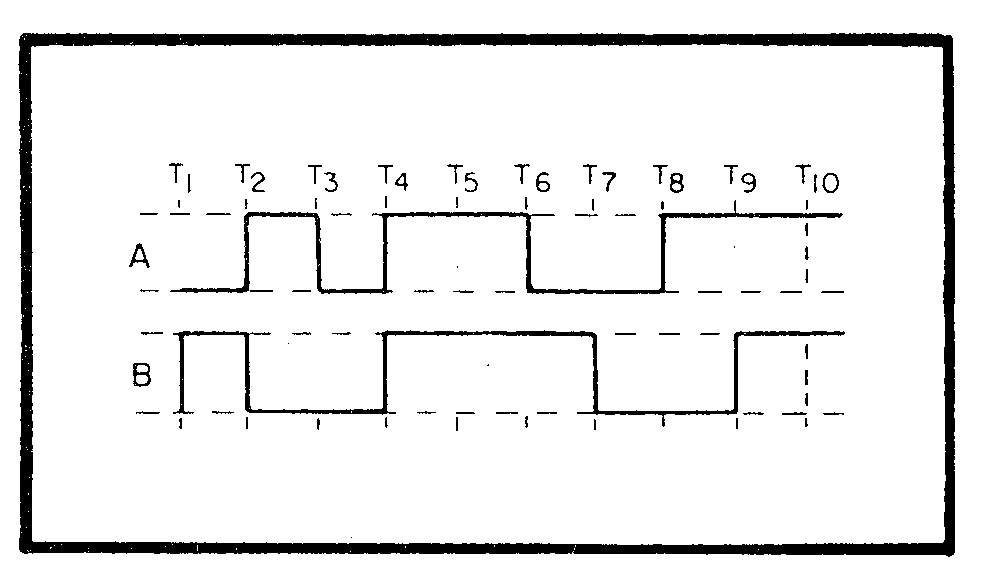
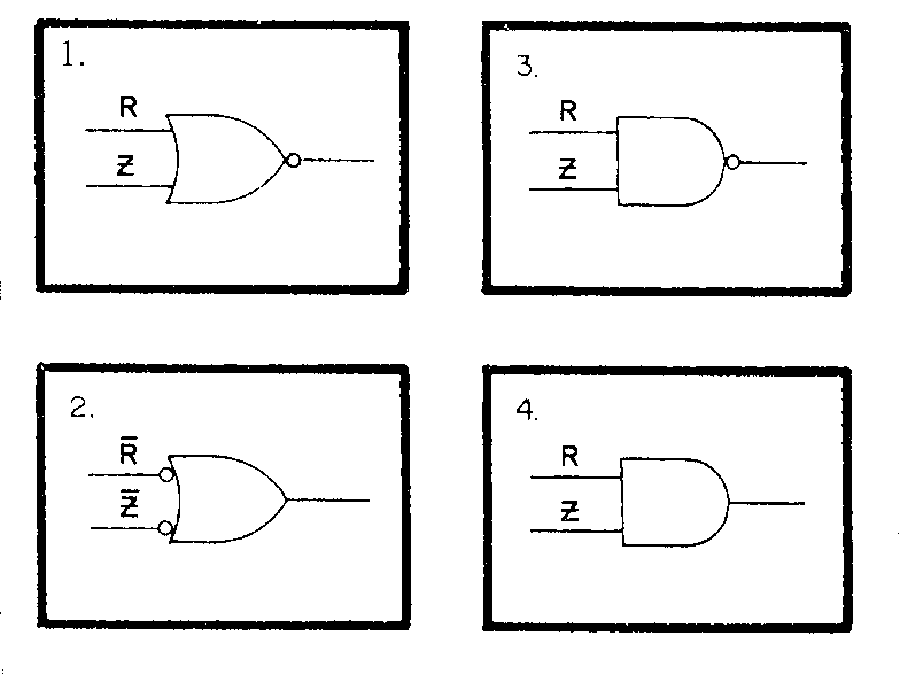
18
3-9. Which of the following logic gates requires all inputs to be TRUE at the same time to produce a TRUE output?
1. OR 2. NOT 3. AND 4. NAND
3-10. Which of the following output Boolean expressions is/are correct for an AND gate?
1. f = AB 2. f = A·B 3. Both 1 and 2 above 4. A=B
3-11. Which of the following symbols represents the output Boolean expression RZ?
Figure 3A. ¾ AND gate timing diagram.
IN ANSWERING QUESTIONS 3-12 THROUGH 3-14, REFER TO FIGURE 3A.
3-12. At which of the following times will the output of a two input AND gate go HIGH?
1. T2, T5, and T8 2. T4 only 3. T2, T6, and T10 4. T4 and T9
3-13. At which of the following times will the output of the AND gate be LOW?
1. T1 to T4 and T5 to T8 2. T1 to T4 and T6 to T9 3. T4 to T6 and T8 to T10 4. T1 to T3 and T6 to T10
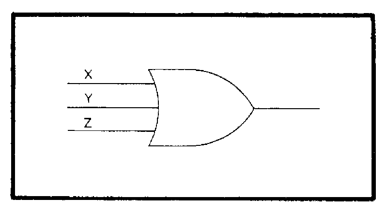
19
3-14. If input B were used instead of input B, how would the output be affected, if at all?
1. It would be HIGH from T2 to T 4 2. It would be LOW from T4 to T 6 3. It would be HIGH from T2 to T 3and
T8 to T9 4. It would not be affected
3-15. What is the output Boolean expression for an AND gate having F, G K, , and L as inputs?
1. f = F G K L 2. f = F + G K L 3. f = F G K L 4. f = F G K L+
THIS SPACE LEFT BLANK INTENTIONALLY.
Figure 3B. ¾ Logic symbol diagram.
IN ANSWERING QUESTIONS 3-16 THROUGH 3-18, REFER TO FIGURE 3B.
3-16. Which of the following gates is represented by the symbol in the figure?
1. AND 2. OR 3. NOR 4. X-OR
3-17. What is the output Boolean expression for the gate?
1. X, Y+Z 2. X+Y ¯ X 3. X+Y+Z 4. X ¯ Y¯ Z
THIS SPACE LEFT BLANK INTENTIONALLY.
20
3-18. Which of the following Truth Tables correspond to the gate in the figure?
1.
X Y Z f
0 0 0 0
0 0 1 1
0 1 0 1
0 1 1 1
1 0 0 1
1 0 1 1
1 1 0 1
1 1 1 1
2.
X Y Z f
0 0 0 0
0 0 1 0
0 1 0 0
0 1 1 1
1 0 0 0
1 0 1 1
1 1 0 1
1 1 1 1
3.
X Y Z f
0 0 0 0
0 0 1 1
0 1 0 1
0 1 1 0
1 0 0 1
1 0 1 0
1 1 0 0
1 1 1 1
4.
X Y Z f
0 0 0 0
0 0 1 1
0 1 0 1
0 1 1 1
1 0 0 0
1 0 1 1
1 1 0 1
1 1 1 1
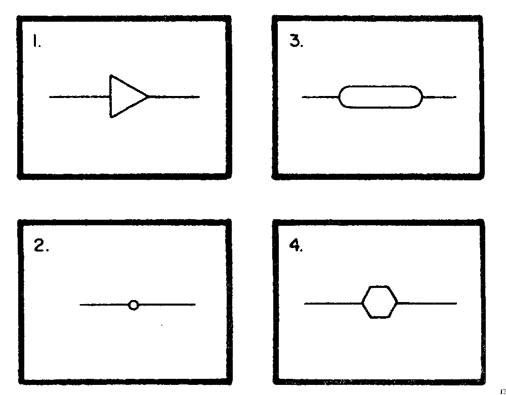
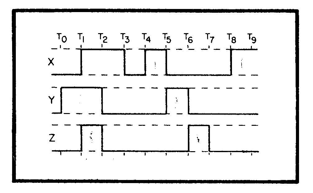
21
Figure 3C. ¾ OR gate timing diagram.
IN ANSWERING QUESTIONS 3-19 THROUGH 3-21, REFER TO FIGURE 3C.
3-19. The gate will have a HIGH output at which of the following times?
1. T0 to T3, T4 to T7, and T8 to T9 2. T1 to T2 and T4 to T9 3. T3 to T4 and T7 to T8 4. T1 to T2 only
3-20. What are the input logic states between T5 and T6?
1. X = 1, Y = 0, Z = 0 2. X = 1, Y = 0, Z = 1 3. X = 0, Y = 1, Z = 0 4. X = 0, Y = 1, Z = 1
3-21. Between T0 and T6, at what times will the output of the gate be LOW?
1. T3 to T4 2. T2 to T5 3. T3 to T6 4. T0 to T1
3-22. What is the Boolean expression for an OR gate having the following inputs?
T (LOW) R (LOW) P (HIGH)
1. T R P 2. T R P 3. T + R + P 4. T + R + P
3-23. What is the purpose of an inverter?
1. To change logic polarity 2. To change voltage levels 3. To amplify the input 4. To complement the input
3-24. Which of the following symbols represents an inverter?
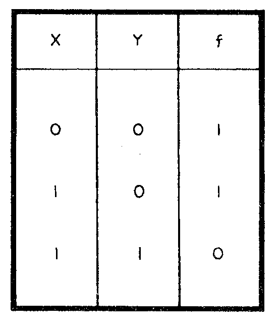
22
3-25. Which of the following is the standard logic symbol for a NAND gate?
3-26. What is the output expression for an inverter with the following input?
(R Q ) + ( S T)
1. ( QR ) + (S T ) 2. R Q S T 3. RQST 4. T)S()Q(R +
3-27. Which of the following gates produces a HIGH output when any or all of the inputs are LOW?
1. AND 2. OR 3. NAND 4. NOR
Figure 3D. ¾ Incomplete NAND gate Truth Table.
IN ANSWERING QUESTION 3-28, REFER TO FIGURE 3D.
3-28. Which of the following NAND gate input combinations and output function is missing?
1. X = 0, Y = 1, f = 0 2. X = 0, Y = 1, f = 1 3. X = 0, Y = 0, f = 0 4. X = 1, Y = 1, f = 1
3-29. What is the output Boolean expression for a NAND gate with inputs G, K, and P ?
1. GK P 2. GKP 3. PGK 4. G K P
23
3-30. The output of a NOR gate will be HIGH under which of the following conditions?
1. When all inputs are HIGH 2. When all inputs are LOW 3. When one input is HIGH 4. When one input is LOW
3-31. What is the output Boolean expression for a NOR gate with P , Q, and R as inputs?
1. RQP ++ 2. RQP ++ 3. RQP ++ 4. RQP ++
Figure 3E. ¾ Input signal timing diagram.
IN ANSWERING QUESTIONS 3-32 THROUGH 3-34, REFER TO FIGURE 3E.
3-32. Figure 3E represents the input signals to a NOR gate. What is the output expression?
1. M + N 2. NM + 3. NM + 4. NM +
3-33. At which of the following times will the output be HIGH?
1. T3 to T4 2. T8 to T9 3. T4 to T6 and T7 to T8 4. T3 to T4 and T8 to T9
3-34. What should the output be between times T3 and T4?
1. LOW 2. HIGH
Figure 3F. ¾ Logic gates.
IN ANSWERING QUESTIONS 3-35 THROUGH 3-37, REFER TO FIGURE 3F.
3-35. What is the output expression for gate D?
1. ZX + 2. XZ 3. ZX + 4. ZX +
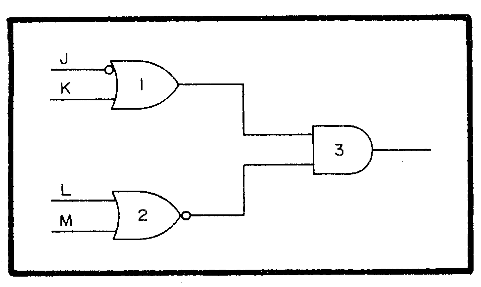
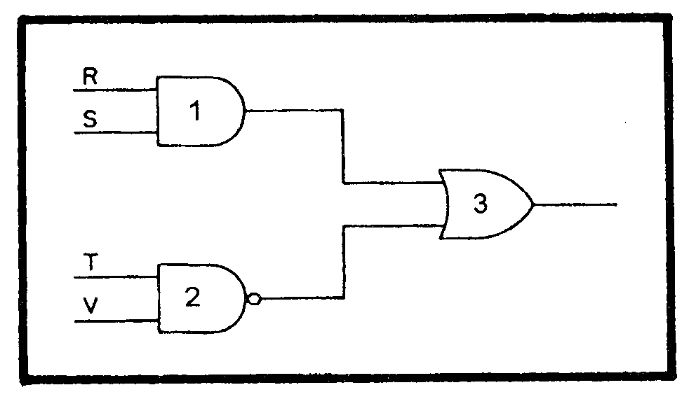
24
3-36. The Truth Tables are identical for which two gates?
1. C and D 2. A and D 3. B and C 4. A and B
3-37. Which gate represents the output
expression ZX ?
1. A 2. B 3. C 4. D
Figure 3G. ¾ Logic circuit.
IN ANSWERING QUESTION 3-38, REFER TO FIGURE 3G.
3-38. Which of the following output expressions represents the output of gate 3?
1. (RS) (TV) 2. RS + TV 3. (RS) + ( TV ) 4. ( RS ) +(TV)
Figure 3H. ¾ Logic circuit.
IN ANSWERING QUESTIONS 3-39 AND 3-40, REFER TO FIGURE 3H.
3-39. The output expression JK represents the output of which, if any, of the following gates?
1. 1 2. 2 3. 3 4. None of the above
3-40. What is the output expression for gate 3?
1. ML(KJ + ) 2. )ML()KJ( ++ 3. )ML()KJ( +++ 4. )ML)(1J(K +
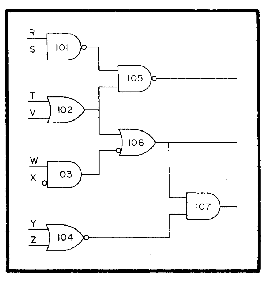
25
Figure 3I. ¾ Logic circuit.
IN ANSWERING QUESTIONS 3-41 THROUGH 3-45, REFER TO FIGURE 3I.
3-41. What is the output expression for gate 105?
1. ( )VT()RS ++ 2. RSTV
3. )VT)(RS( + 4. )VT()RS( ++
3-42. Which of the following gates provides a common output to two other gates?
1. 101 2. 102 3. 104 4. 106
3-43. Which of the following expressions represents the output of gate 106?
1. TVXW 2. VTXW +++ 3. )XW()TV( + 4. )XW(V)(T ++
3-44. Which of the following conditions will cause gate 107 output to be HIGH?
1. Gate 106 is LOW; Y and Z are HIGH
2. Gate 106 is LOW; Y is HIGH, Z is LOW
3. Gate 106 is HIGH; Y and Z are LOW
4. Gate 106 is HIGH; Y is LOW, Z is HIGH
3-45. What is the output expression for gate 107?
1. )ZY)(XWTV( ++ 2. ( XWVT +++ )(YZ) 3. ((T+V)+( W +X))( YZ ) 4. )ZY)(XW)(VT( ++
3-46. Boolean algebra is used primarily by which of the following groups?
1. Fabricators 2. Technicians 3. Design engineers 4. Repair personnel
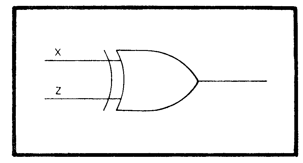
26
3-47. Which of the following Boolean laws states, "a term that is TRUE in one part of an expression will be TRUE in all parts of the expression"?
1. Identity 2. Commutative 3. Complementary 4. Double negative
3-48. The examples AB = BA and A+B = B+A represent which of the following Boolean laws?
1. Associative 2. Commutative 3. Intersection 4. Union
3-49. What type of logic gate is modified to produce an exclusive OR gate?
1. AND 2. NAND 3. OR 4. NOR
3-50. Which of the following symbols represents the operation function of an exclusive OR gate?
1. Q 2. ¯ 3. O 4. ˜
Figure 3J. ¾ Logic gate.
IN ANSWERING QUESTIONS 3-51 AND 3-52, REFER TO FIGURE 3J.
3-51. What will be the output of the gate when (a) X is HIGH and Z is LOW, and (b) X and Z are both HIGH?
1. (a) LOW (b) LOW 2. (a) LOW (b) HIGH 3. (a) HIGH (b) LOW 4. (a) HIGH (b) HIGH
3-52. What will be the output of the gate when (a) X and Z are both LOW and (b) X is LOW and Z is HIGH?
1. (a) LOW (b) LOW 2. (a) LOW (b) HIGH 3. (a) HIGH (b) LOW 4. (a) HIGH (b) HIGH
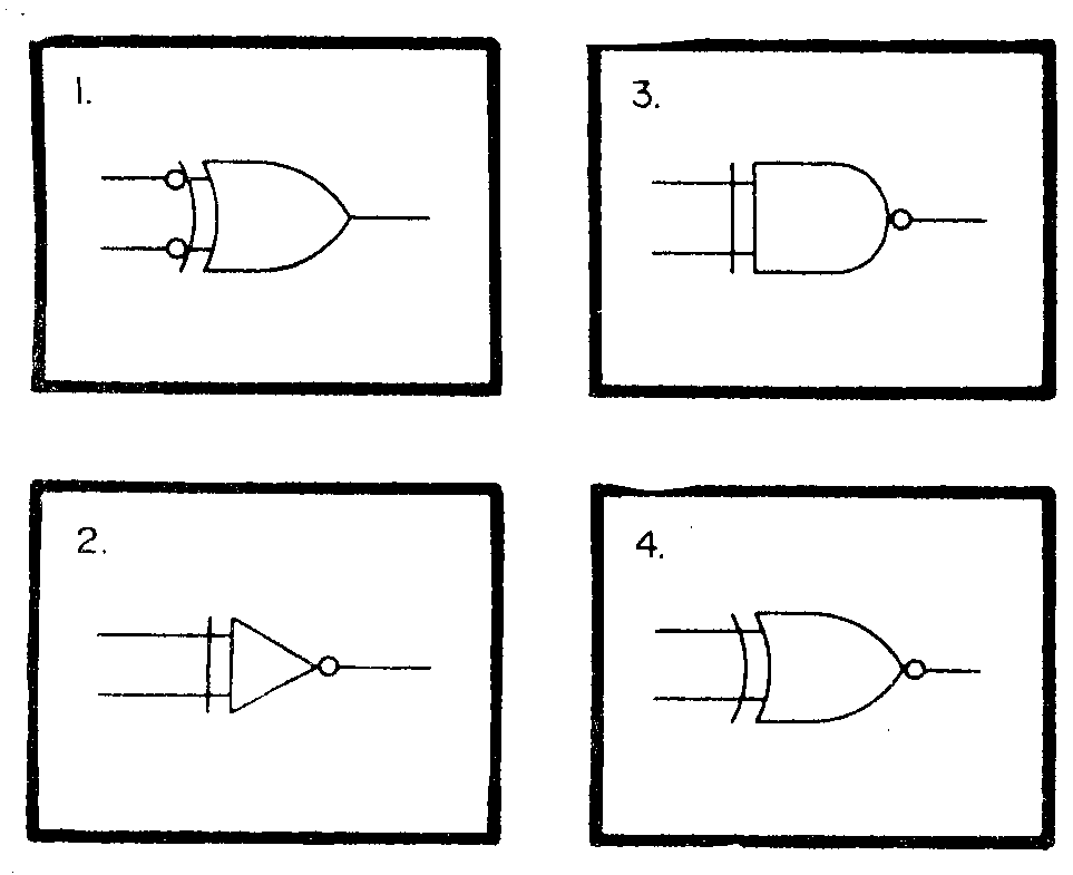
27
3-53. Which of the following symbols represents an exclusive NOR gate?
3-54. What is the output of an exclusive NOR gate when (a) all inputs are LOW and (b) all inputs are HIGH?
1. HIGH (b) HIGH 2. LOW (b) HIGH 3. HIGH (b) LOW 4. LOW (b) LOW
3-55. What is the output expression for an exclusive NOR gate with R and T as inputs?
1. TR ¯ 2. TR + 3. TR + 4. TR ¯
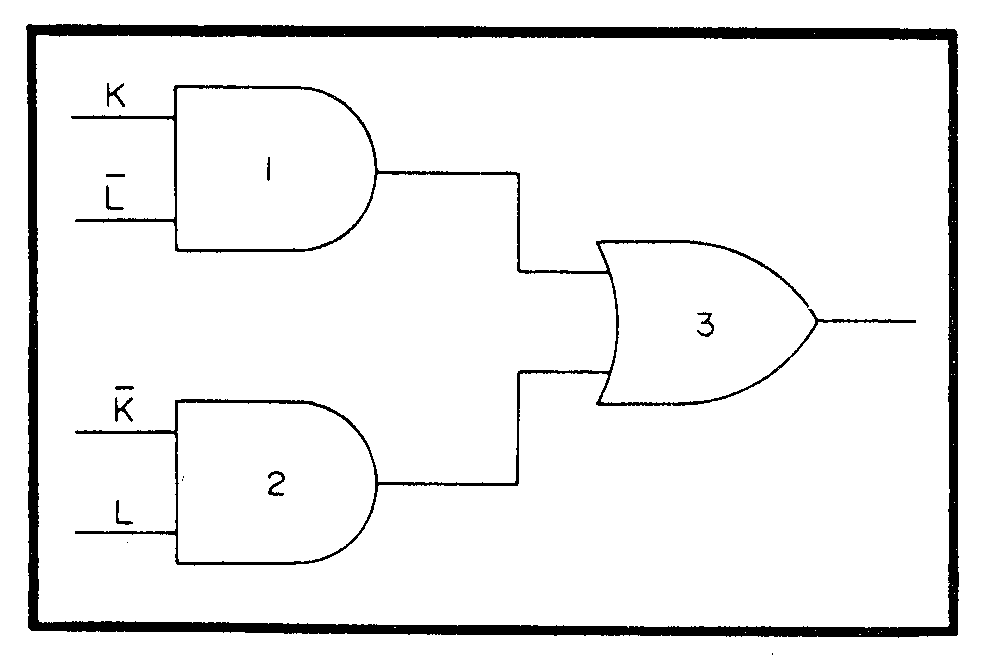
28
ASSIGNMENT 4 Textbook assignment: Chapter 4, “Special Logic Circuits,” pages 3-3 through 3-67.
________________________________________________________________________________
4-1. Which of the following circuits will add two binary digits but not produce a carry?
1. AND gate 2. Half adder 3. Quarter adder 4. Summation amplifier
Figure 4A.—Logic circuit.
IN ANSWERING QUESTIONS 4-2 THROUGH 4-5, REFER TO FIGURE 4A.
4-2. What type of circuit is depicted in the
figure?
1. Inverter amplifier 2. Half subtracter 3. Half adder 4. Quarter adder
4-3. Which of the following gates will have
HIGH outputs when K is HIGH and L is LOW?
1. 1 only 2. 3 only 3. 1 and 2 4. 1 and 3
4-4. What will be the output of gate 3 when
K and L are both HIGH?
1. LOW 2. HIGH
4-5. Assume that K and L are both HIGH.
Which of the following statements represents the output of gate 3?
1. 1 plus 1 = 0 (No carry) 2. 1 plus 0 = 1 3. 0 plus 1 = 1 4. 0 plus 0 = 0
4-6. Which of the following gates performs
the same function as a quarter adder?
1. Half adder 2. Exclusive OR 3. NOR 4. Exclusive NOR
THIS SPACE LEFT BLANK INTENTIONALLY.
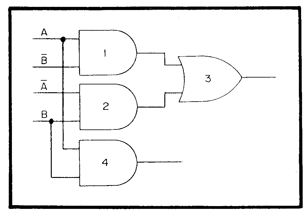
29
Figure 4B.—Logic circuit.
IN ANSWERING QUESTIONS 4-7 THROUGH 4-9, REFER TO FIGURE 4B.
4-7. Which of the following circuits is shown
in the figure?
1. Quarter adder 2. Half adder 3. Full adder 4. Subtracter
4-8. Which of the following gate
combinations may be replaced with an exclusive OR gate?
1. 1, 2, and 3 2. 1, 2, and 4 3. 1, 3, and 4 4. 2, 3, and 4
4-9. The output of gate 3 is the (a) and the
output of gate 4 is the (b).
1. (a) Carry (b) sum 2. (a) Sum (b) difference 3. (a) Sum (b) carry 4. (a) Carry (b) difference
4-10. What is the largest sum that can be obtained from a half adder?
1. 012 2. 102 3. 112 4. 1002
4-11. Which of the following statements describes the difference between a half adder and a full adder?
1. A half adder produces a carry 2. A full adder produces a carry 3. A half adder will add a carry from
another circuit 4. A full adder will add a carry from
another circuit
THIS SPACE LEFT BLANK INTENTIONALLY.
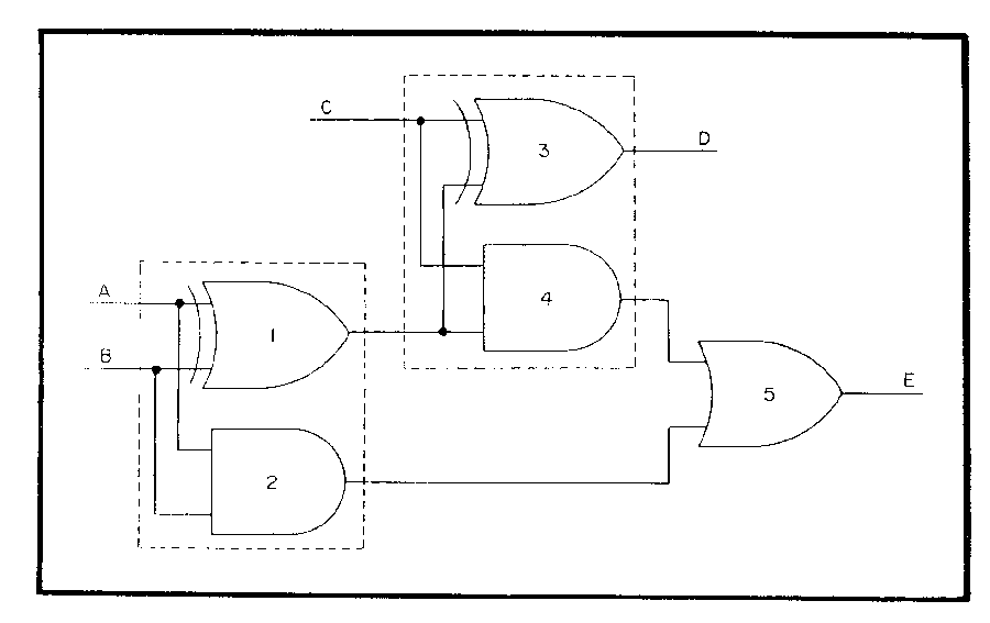
30
Figure 4C.—Logic circuit.
IN ANSWERING QUESTIONS 4-12 THROUGH 4-14, REFER TO FIGURE 4C.
4-12. What type of circuit is shown in the
figure?
1. Full adder 2. Subtracter adder 3. Double half adder 4. Double exclusive OR
4-13. If A and B are 0 and C is 1, what will be
the outputs at D and E?
1. D = 0, E = 0 2. D = 0, E = 1 3. D = 1, E = 0 4. D = 1, E = 1
4-14. Under which of the following conditions will outputs D and E both be HIGH?
1. A, B, and C are HIGH 2. A and B are HIGH, C is LOW 3. A and B are LOW, C is HIGH 4. A, B, and C are LOW
4-15. What is the largest sum that can be
obtained from a full adder?
1. 102 2. 112 3. 1002 4. 1112
4-16. How many full adders are required to
form a parallel adder capable of adding 100012 and 10002?
1. Five 2. Six 3. Three 4. Four
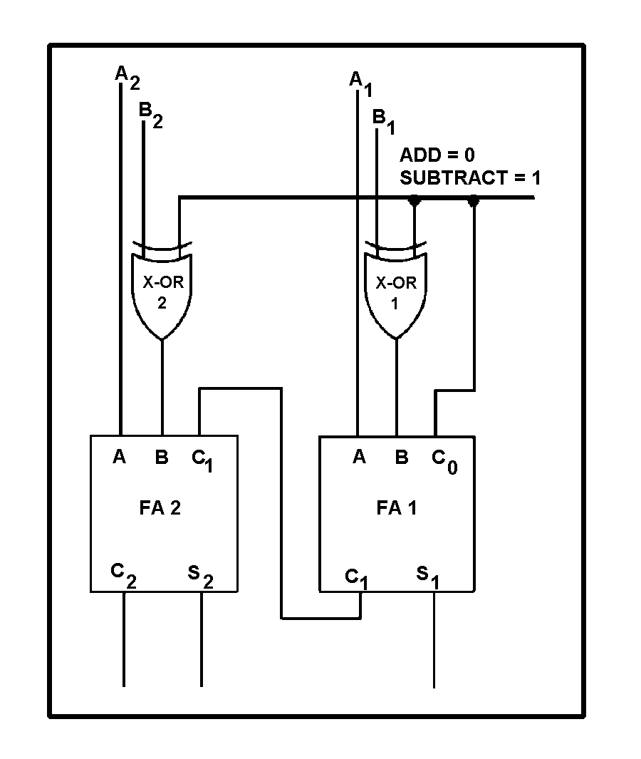
31
4-17. Which of the following statements describes the method used in computers to subtract binary numbers?
1. R's complement the minuend and
add to the subtrahend 2. Add the minuend and subtrahend
and complement the sum 3. R's complement the subtrahend and
add to the minuend 4. Subtract the subtrahend from the
minuend and complement the difference
Figure 4D.—Adder/subtracter circuit.
IN ANSWERING QUESTIONS 4-18 THROUGH 4-20, REFER TO FIGURE 4D.
4-18. What type of complement is performed
by X-OR gates 1 and 2?
1. R's complement 2. Minuend complement 3. R's + 1 complement 4. Difference complement
4-19. Which of the following inputs is used for the least significant digit of the minuend?
1. A1 2. A2 3. B1 4. B2
4-20. What will be the output of (a) X-OR 2
and (b) X-OR 1 in the subtract mode with a subtrahend of 102?
1. (a) 0 (b) 0 2. (a) 0 (b) 1 3. (a) 1 (b) 0 4. (a) 1 (b) 1
4-21. Flip-flops are what type of
multivibrators?
1. Astable 2. Monostable 3. Free running 4. Bistable
4-22. Flip-flops may NOT be used for which
of the following operations?
1. Temporary storage 2. Subtraction 3. Division 4. Transfer of information
4-23. When, if ever, will the outputs Q and Q of an R-S flip-flop be the same?
1. When R and S are both LOW 2. When R is LOW and S is HIGH 3. When R is HIGH and S is LOW 4. Never
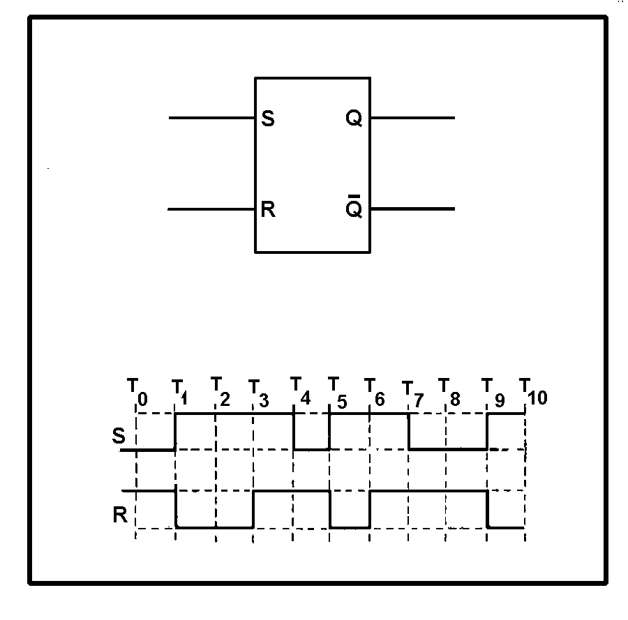
32
Figure 4E.—R-S flip-flop with timing diagram.
WHEN ANSWERING QUESTIONS 4-24 AND 4-25, REFER TO FIGURE 4E.
4-24. Assume the flip-flop is set at T0. At
which of the following times will the flip-flop be reset?
1. T1 to T3, T5 to T6, and T9 to T10 2. T0 to T1, T3 to T5, and T6 to T9 3. T1 to T3, T5 to T7, and T9 to T10 4. T1 to T4, T5 to T7, and T9 to T10
4-25. What happens to the flip-flop at T6?
1. It sets 2. It resets 3. It sets and immediately resets 4. It remains reset
4-26. Which of the following statements
describes a toggle flip-flop?
1. A monostable device 2. An astable device that changes state
only on a set pulse 3. A two input bistable device 4. A bistable device with a single input
4-27. A T flip-flop is used primarily for which of the following functions?
1. To divide the input frequency by
two 2. To double the input frequency 3. To amplify the input frequency 4. To invert the input frequency
4-28. What are the inputs to a D flip-flop?
1. Set and reset 2. Set and clock 3. Data and clock 4. Reset and data
4-29. What is the purpose of a D flip-flop?
1. To eliminate the output of the
equipment 2. To divide the data input by the clock
frequency 3. To store data until it is needed 4. To toggle the data input
4-30. An inverter on the clock input has which
of the following effects on the D flip- flop?
1. The output will change on the
negative-going transition of the clock pulse
2. The output will change on the positive-going transition of the clock pulse
3. The data input will change at the clock frequency
4. The output will change at the clock frequency
4-31. Which of the following statements is
true concerning CLR and PR pulses to the D flip-flop?
1. CLR causes Q to go high, PR causes
Q to go low 2. CLR and PR override any existing
output condition 3. Other inputs override CLR and PR 4. CLR and PR have no effect on the
output
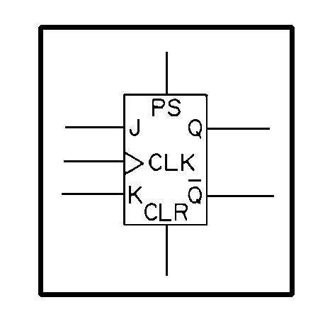
33
4-32. Which of the following statements is correct concerning D flip-flops?
1. The output is delayed up to one
clock pulse 2. Input data is delayed until it
coincides with the clock 3. The clock is delayed until it
coincides with the input data 4. The output is always a square wave
Figure 4F.—Standard symbol for a J-K flip-flop.
WHEN ANSWERING QUESTIONS 4-33 THROUGH 4-36, REFER TO FIGURE 4F.
4-33. The flip-flop shown in the figure may be
used in place of which of following flip- flops?
1. R-S 2. T 3. D 4. Each of the above
4-34. With the clock applied and J and K inputs held HIGH, what is the output at Q?
1. Constant HIGH 2. Constant LOW 3. Toggle at one half the clock
frequency 4. Toggle at twice the clock frequency
4-35. What will be the Q output if K is HIGH and CLK goes HIGH?
1. HIGH 2. LOW
4-36. A pulse on which of the following
inputs will cause the flip-flop to set regardless of the other inputs?
1. CLK 2. CLR 3. J or K 4. PR or PS
4-37. The circuit which generates a timing
signal to control operations is called a/an
1. clock 2. counter 3. oscillator 4. bistable multivibrator
4-38. Which of the following statements is
true regarding astable multivibrators used as clocks?
1. As multivibrator frequency
increases, stability decreases 2. Output 2 will have a higher voltage
than output 1 3. The frequency stability may be
increased by applying a higher frequency trigger
4. A trigger of lower frequency will stabilize the output frequency
4-39. Which of the following types of circuits
will produce a stable clock when triggered by an outside source?
1. R-S flip-flop 2. Bistable multivibrator 3. One-shot multivibrator 4. D flip-flop
34
4-40. Which of the following types of clocks would probably be used in a complex piece of equipment with a variety of timing requirements?
1. Single triggered-monostable 2. Single free-running 3. Triggered-astable for each section of
the equipment 4. Multiphase
4-41. What is the modulus of a 3-stage binary
counter?
1. 7 2. 8 3. 3 4. 4
4-42. Counters may be used for which of the following purposes?
1. Counting operations, quantities and
time 2. Dividing frequency 3. Addressing information in storage 4. Each of the above
THIS SPACE LEFT BLANK INTENTIONALLY
Figure 4G.—Standard symbol circuit.
35
WHEN ANSWERING QUESTIONS 4-43 THROUGH 4-46, REFER TO FIGURE 4G. FOR EACH QUESTION, ASSUME THAT ALL FFs ARE INITIALLY RESET.
4-43. What type of circuit is shown?
1. J-K flip-flops 2. Clock 3. Shift register 4. Ripple counter
4-44. Assume all lights are out. After 6 input
pulses, which two lamps will be lit?
1. A and B 2. A and C 3. B and C 4. B and D
4-45. Assume all lamps are out. After 16 input pulses, which lamps, if any, will be lit?
1. A, B, C, and D 2. B, C, and D 3. A, B, and D 4. None
4-46. What is the main disadvantage of using
this circuit with a high frequency input?
1. The circuit will burn up 2. Possible errors in the output 3. The flip-flops will act as T flip-flops 4. Above a certain frequency the
circuit will count in the opposite direction
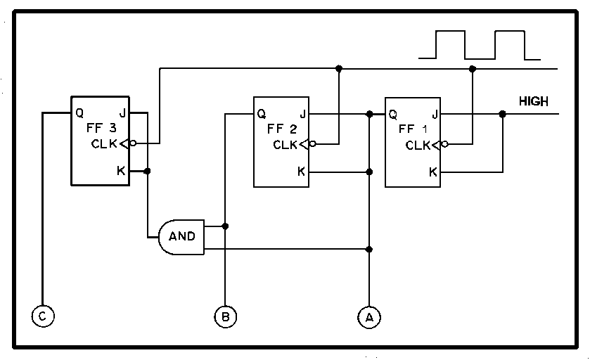
Figure 4H.—Counter circuit.
36
WHEN ANSWERING QUESTIONS 4-47 THROUGH 4-50, REFER TO FIGURE 4H.
4-47. What is the maximum count that this
counter is capable of holding?
1. 58 2. 78 3. 38 4. 48
4-48. What type of counter is shown?
1. Ring 2. Asynchronous 3. Synchronous 4. Decade
4-49. Under which of the following conditions will the output of the AND gate be HIGH?
1. FF 1 and FF 2 are set 2. FF 1 and FF 2 are reset 3. FF 2 and FF 3 are set 4. FF 1 and FF 3 are reset
4-50. With all the FFs initially reset, the AND
gate output will be HIGH after how many input pulses?
1. 3 only 2. 4 only 3. 7 only 4. 3 and 7
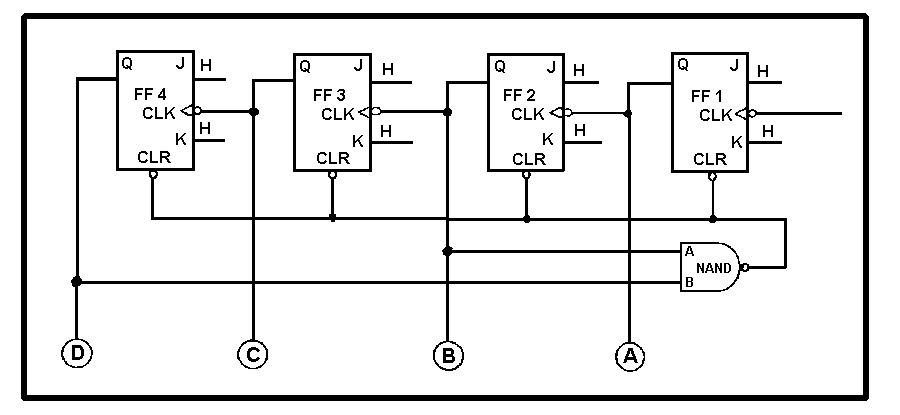
Figure 4I.—Counter circuit.
37
WHEN ANSWERING QUESTIONS 4-51 AND 4-52, REFER TO FIGURE 4I.
4-51. What is the maximum binary count that
will be shown before all the flip-flops reset?
1. 1112 2. 10102 3. 11112 4. 10002
4-52. To change the maximum count from 1010 to 910, which two flip-flops would be wired as NAND gate inputs?
1. FF 1 and FF 2 2. FF 2 and FF 3 3. FF 1 and FF 4 4. FF 1 and FF 3
THIS SPACE LEFT BLANK INTENTIONALLY.
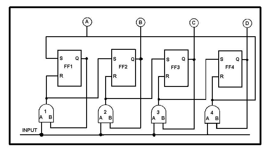
Figure 4J.—Counter circuit.
38
WHEN ANSWERING QUESTIONS 4-53 THROUGH 4-55, REFER TO FIGURE 4J.
4-53. Which of the following types of
counters is shown in the figure?
1. Ring 2. Asynchronous 3. Synchronous 4. Decade
4-54. At any given time, how many flip-flops
may be set?
1. Only one 2. Any two 3. Any three 4. All
4-55. Which of the following conditions must exist to set FF 3?
1. AND gate 1 output HIGH 2. AND gate 2 output HIGH 3. AND gate 3 output LOW 4. Clock input to AND gate 3 LOW
and AND gate 4 output HIGH
THIS SPACE LEFT BLANK INTENTIONALLY
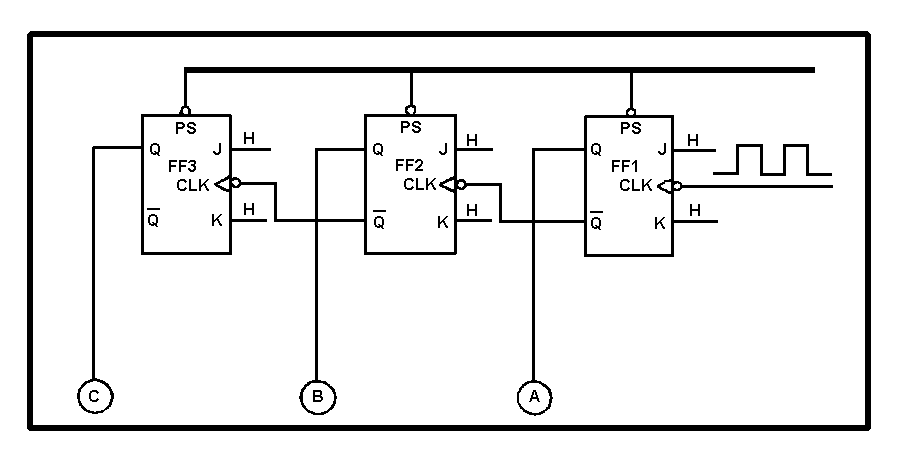
Figure 4K.—Down counter.
39
WHEN ANSWERING QUESTIONS 4-56 AND 4-57, REFER TO FIGURE 4K.
4-56. Assume only FF 1 and FF 3 are set.
Which, if any, of the flip-flops will be set after the next clock pulse?
1. FF 2 only 2. FF 3 only 3. FF 2 and FF 3 4. None
4-57. Assume that all FFs are set, which of the
following actions will take place at clock pulse 4?
1. FF 1, FF 2 and FF 3 will set 2. FF 1 will set, FF 2 and FF 3 will
reset 3. FF 1, FF 2, and FF 3 will reset 4. FF 1 and FF 2 will set, FF 3 will
reset
4-58. What term identifies a series of FFs designed to temporarily store information?
1. Data word 2. Counter 3. Register 4. DIP package
4-59. Which of the following statements
describes parallel transfer?
1. Data is transferred one bit at a time 2. All data bits are transferred
simultaneously 3. Data is received in serial form and
transferred in parallel form 4. Data is transferred on a single line
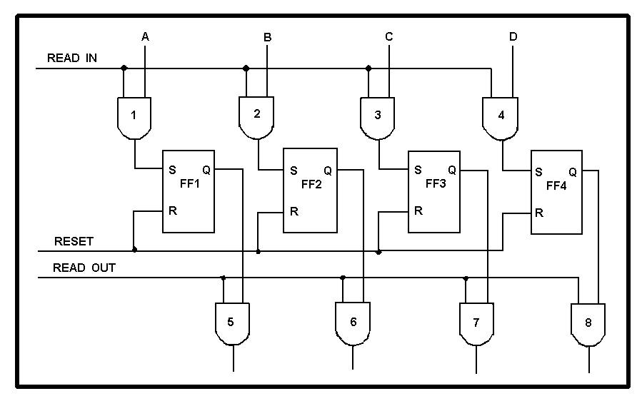
Figure 4L.—Parallel register.
40
WHEN ANSWERING QUESTIONS 4-60 AND 4-61, REFER TO FIGURE 4L.
4-60. Which of the following methods will
clear the register of old information no longer needed?
1. A HIGH applied to the READ IN
line 2. A HIGH applied to the RESET line 3. A LOW applied on the RESET and
a HIGH on the READ OUT lines 4. HIGHs are applied on the A, B, C,
D, and READ IN lines
4-61. Under which of the following conditions will the output of gate 7 be HIGH?
1. When FF 3 and RESET are HIGH 2. When gate 3 and FF 3 are HIGH 3. When FF 3 and READ OUT are
HIGH 4. When the output of gate 3 is HIGH
THIS SPACE LEFT BLANK INTENTIONALLY
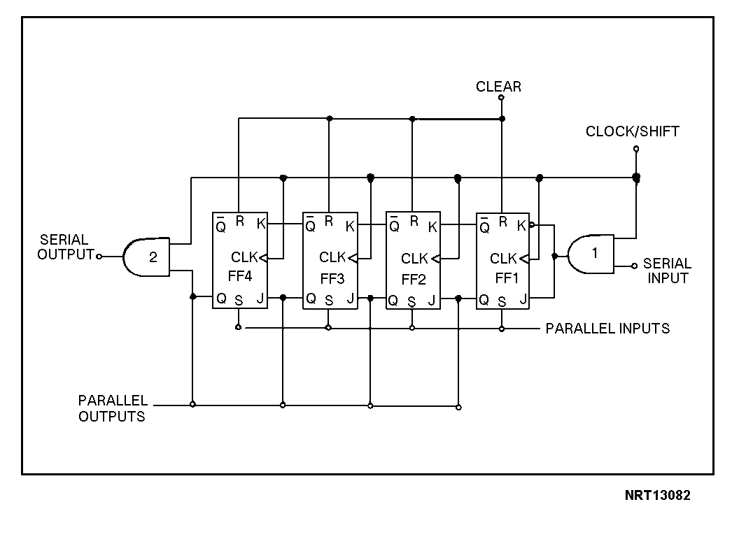
Figure 4M.—Shift register.
41
WHEN ANSWERING QUESTIONS 4-62 THROUGH 4-67, REFER TO FIGURE 4M.
4-62. Which of the following operations is the
circuit capable of performing?
1. Serial-to-parallel conversion 2. Parallel-to-serial conversion 3. Left shifts 4. Each of the above
4-63. What is the maximum word length the
register is capable of handling?
1. 6 bit 2. 5 bit 3. 3 bit 4. 4 bit
4-64. How many clock/shift pulses are required to serially input a word into the register?
1. 1 2. 5 3. 3 4. 4
4-65. To output a word in parallel form, how
many output lines are required?
1. 1 2. 2 3. 4 4. 8
42
4-66. To increase the value of a word by one power of 2, how many shifts are required?
1. 1 2. 2 3. 3 4. 0
4-67. Which of the following operations takes
the longest time?
1. Serial in, parallel out 2. Serial in, serial out 3. Parallel in, serial out 4. Parallel in, parallel out
4-68. Shifting a word in a shift register 3
places to the left is equal to multiplying the number by how much?
1. 1010 2. 210 3. 810 4. 410
4-69. Logic families are identified by which of the following means?
1. Logic polarity required 2. The types of elements used 3. Size and cost of manufacture 4. Packaging (DIP, TO, flat packs)
4-70. A TTL logic circuit would use which of
the following types of elements?
1. Diode-transistor 2. Resistor-transistor 3. Transistor-transistor 4. Complementary metal oxide